8085 microprocessor
8085 microprocessor. Features. 8 bit microprocessor( 8085 microprocessor can read or write or perform arithmetic and logical operations on 8-bit data at time ) It has 8 data lines and 16 address lines hence capacity is 216 = 64 kB of memory Cock frequency is 3 MHz

8085 microprocessor
E N D
Presentation Transcript
Features • 8 bit microprocessor(8085 microprocessor can read or write or perform arithmetic and logical operations on 8-bit data at time) • It has 8 data lines and 16 address lines hence capacity is 216 = 64 kB of memory • Cock frequency is 3 MHz • It requires +5V power supply. • It is a single chip NMOS device implemented with 6200 transistors. • It provides 74 instructions with five addressing modes. • It provides 5 hardware interrupt and 8 software interrupts.
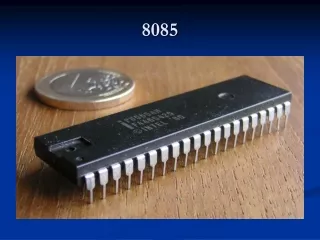
Pin Configuration • 40 pins classified into 6 groups: • Data bus • Address bus • Control & status lines • Externally generated • Serial interface • Power supply & clock
Pin Configuration cont… 1) Address Bus (A15-A8 and AD7-AD0): The microprocessor 8085 has 16 bit address lines from A15-A8 and AD7-AD0. These lines are used to transfer 16 bit address of memory as well as 8-bit address of I/O ports. 2) Data Bus: The lower 8 lines (AD7-AD0) are often called as multiplexed data lines.
CONTROL LINES • RD : Read: This is active low signal which indicates that the selected I/O or memory device is to be read and also is available on the data bus. • WR : Write: This is active low signal which indicates that the data on data bus are to be written into a selected memory location. • IO/ M : (Input / Output / Memory): This is used to select either Input / Output devices or memory operation. When it is high it indicates an I/O operation and when it is low, it indicates a memory operation. STATUS LINES • Status Pins (S1, S0): The microprocessor 8085 has two status pins as S1, S0 which is used to indicate the status of microprocessor or operation which is performed by microprocessor.
SPECIAL SIGNAL • ALE (Address Latch Enable): The ALE signal is used to enable or disable the external peripherals (LATCH). • The external latch IC is used for the de-multiplexing of AD7-AD0 lines, i.e., it is used to separate the address and data from AD7-AD0 lines. • If ALE = 1/0 then external latch IC is enabled / disabled respectively.
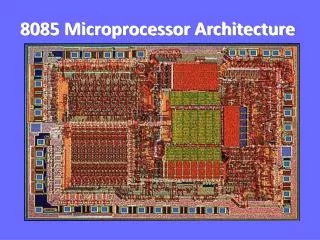
ALU • Timing and Control Unit • General Purpose Registers • Program Status word • Program Counter • Stack Pointer • Instruction Register and Decoder 8. Interrupt Control 9.Serial I/O Control 10.Address Bus 11. Data Bus Architecture 0f 8085 Cont…
REGISTERS The Registers are of 8-bit & 16-bit size used for different purposes A- Accumulator – This is an special purpose register. All the ALU operations are performed with reference to the contents of Accumulator. B,C,D,E,H,L – General purpose registers. These registers can also used for 16-bit operations in pairs. The default pairs are BC, DE & HL.
F – Flag register – This register indicates the status of the ALU operation. PC – Program Counter – This is a 16-bit register used to address the memory location from where an instruction is going to be executed.
SP – Stack pointer - This is a 16-bit register used to address the top of the stack memory location. • Temporary register, W & Z – These registers are only used by 8085 and are not available for the programmer.
ALU – Arithmetic & Logic Unit • ALU of 8085 performs 8-bit arithmetic & logical operations. The operations are generally performed with Accumulator as one of the operands. The result is saved in accumulator register. • Timing & Control Unit • This unit works as the brain of the CPU and generates all the timing and control signals to perform all the internal & external operations of the CPU. • Instruction Decoder & Machine Cycle Encoder Unit • This unit decodes the op-code stored in the Instruction Register (IR) and encodes it for the timing & control unit to perform the execution of the instruction.
The 8085 Bus Structure The 8-bit 8085 CPU (or MPU – Micro Processing Unit) communicates with the other units using a 16-bit address bus, an 8-bit data bus and a control bus.
Over all structure Chip Selection Circuit A15- A10 8085 CS A15-A8 ALE A9- A0 1K Byte Memory Chip AD7-AD0 Latch A7- A0 D7- D0 WR IO/M RD WR RD
MPU Communication and Bus Timing Figure 3: Moving data form memory to MPU using instruction MOV C, A (code machine 4FH = 0100 1111)
Instruction Set • Broadly classified into two types: • Based on size: • One Byte - Opcode only (CMA, ADD B) • Two Byte - Opcode ,an operand (MVI A,32H) • Three Byte - Opcode, operand, operand (LDA 4200, STA 4500) • Based on function: • Data transfer group (MOV A,B; MVI A,32H;MOV C,4500) • Arithmetic operations (ADD B, SBI 32H,INC D, DEC B) • Logical operations (ANA B, ORI 05H, RLC, RAR) • Branching operations (JMP, JNZ, JC, CALL, RETURN) • Machine control instructions (HLT, NOP,EI,DI,SIM,RIM)
ADDRESSING MODES • Immediate (MOV A,B ;ADD B; SUB E;ANA C) • Register (MVI A,05H;LXI B, 20AEH; ADI 05H;ORI 07H) • Direct (LDA 4500H;STA 7500H;IN 09H;OUT 70H) • Indirect (MOV A, M;MOV M,A;ADD M;ORA M) • Implied(implicit) (HLT; NOP;RST;RET)
Timing diagrams • The 8085 microprocessor has 7 basic machine cycle. They are 1. Op-code Fetch cycle(4T or 6T). 2. Memory read cycle (3T) 3. Memory write cycle(3T) 4. I/O read cycle(3T) 5. I/O write cycle(3T) 6. Interrupt Acknowledge cycle(6T or 12T) 7. Bus idle cycle
8-BIT ADDITION & SUBTRACTION Program: MVI A, 04H MVI B, 06H MVI C, 00H ADD B JNC LP1 INR C LP1: STA 4500H MOV A, C STA 4501H HLT Program: MVI A, 06H MVI B, 04H MVI C, 00H SUB B JNC LP1 INR C LP1: STA 4500H MOV A, C STA 4501H HLT
8 BIT MULTIPLICATION MVIA, 00 H MVIB, 05 H MVID, 04 H MVIC, 00 H *ADD B JNC # INR C # DCR D JNZ * STA 9000 H MOV A, C STA 9001 H HLT
8 BIT DIVISION MVIA, 04 H MVIB, 02 H MVIC, 00 H #SUB B INR C JNC # ADD B DCR C STA 9000 H MOV A, C STA 9001 H HLT
16 –BIT ADDITION &SUBTRATION: Program: MVI B, 00 H LXI H, 2222 H LXI H, 1111 H MOV A, L SUB E MOV L, A MOV A, H SBB D JNC # INR B #MOV H, A SHLD 9000 H MOV A, B STA 9002 H HLT Program: MVI B, 00 LXI H, 1111 H LXI D, 2222 H MOV A, L ADD E MOV L, A MOV A, H ADC D JNC # INR B # MOV H, A SHLD 9000 H MOV A, B STA 9002 H HLT
16 –BIT MULTIPLICATION & DIVISION Program: LXI B, 0000 H LHLD 9002 H XCHG LHLD 9000 H $INX B MOV A, L SUB E MOV L, A MOV A, H SBB D MOV H, A SBB D MOV H, A JNC $ DAD D DCX B SHLD 9100 H MOV L, C MOV H, B SHLD 9102 H HLT Program: LXI B, 0000 H LHLD C100 H SPHL LHLD C102 H XCHG LXI H, 0000 H @ DAD SP JNC * INX B *DCX D MOV A, D ORA E JNZ @ SHLD 9000 H MOV L, C MOV H, B SHLD 9002 H HLT
To find the greatest between two numbers: Program MVI B, 30H MVI C, 40H MOV A, B CMP C JZ EQU JC GRT OUT PORT1 HLT EQU: MVI A, 01H OUT PORT1 HLT GRT: MOV A, C OUT PORT1 HLT
Code conversion • ASCII to decimal • Decimal to ACSII • BCD to HEXA • Hexa to BCD • Hexato binary

