Download
1 / 16
160 likes | 308 Vues
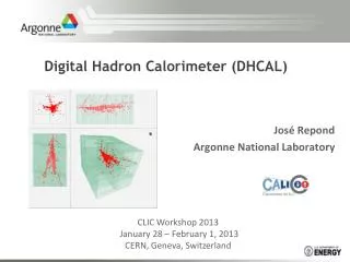
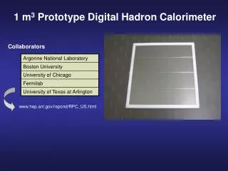
1 m 3 Prototype Digital Hadron Calorimeter. Collaborators. www.hep.anl.gov/repond/RPC_US.html. New Concept of Digital Hadron Calorimeter. Traditional calorimeter. Small number (~10 5 ) of readout channels. Large number (10 – 18) of bits per channel. +. =.

E N D
1 m3 Prototype Digital Hadron Calorimeter Collaborators www.hep.anl.gov/repond/RPC_US.html
New Concept of Digital Hadron Calorimeter Traditional calorimeter Small number (~105) of readout channels Large number (10 – 18) of bits per channel + = Excellent single particle resolution ECAL: large number of bits per channel HCAL: small number (1 – 2) of bits per channel Large number (~108) of readout channels + Digital hadron calorimeter = Reduces ‘confusion’ term Preserves single particle (hadrons) resolutions
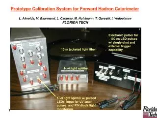
Development of the Readout Electronics 40 layers à 1 m2 Real challenge 400,000 readout channelsCheap (≤ 1$/channel) 1 cm2 readout pads Low cross-talk, noise… Conceptual design of system I Front-end ASIC II Data concentrator III VME data collection IV Trigger and timing system
Front-end ASIC 64 inputs with choice of input gains RPCs (streamer and avalanche), GEMs… Triggerless or triggered operation 100 ns clock cycle Output: hit pattern and time stamp ASIC performance specified in 41 page document
ASIC design work at FNAL Abderrezak Mekkaoui James Hoff FNAL Ray Yarema First design meeting between ANL and FNAL in February Design work started in June First submission hopefully in CY2004 Pictures of chip layout and data structure by James Hoff
Analog circuitry taken from recently built FSSR chip (BTeV) Only one gain setting Modifications not before CY2005 Chip has data indicator essentially a fast OR Hit catcher with possibility to mask noisy channels 32 Inputs 32 Inputs Digital IO
Timestamp resets every 1 second unique value for clock speed of 10 MHz Pipeline to accommodate trigger decision can be removed in triggerless operation Write out buffer
0 T7 D7 S7 S6 0 T6 D6 0 D5 S5 T5 D4 0 S4 T4 D3 T3 0 S3 D2 S2 T2 0 0 D1 T1 S1 T0 D0 S0 0 0 1 1 0 1 0 0 1 1 1 1 1 Output word structure Sync Word Bit Zero Status Word Time Word Data Word
S7 S6 S5 S4 S3 S2 S1 S0 1 1 1 The Status Word
Ordinary Data I/O Operation Sync Word Status Word Sync Word Status Word 1 Time Slice 1 Time Slice 1 Time Slice 1 Time Slice
When a TimeSlice is triggered Sync Word Status Word Sync Word Data Frame 1 Time Slice 12 Time Slices 1 Time Slice 1 Time Slice
The Data Frame 11 bits x 11 words
ASIC Development Concept Realization Verilog Schematic Layout Digital Simulations SPICE Simulations Port Lay-out Simulations
Status of Design Effort As of July 25, 2004 Goal: first submission in October, 2004
Time scales R&D with chambers Essentially completed Electronic readout system Design and prototype ASIC Specify entire readout system Prototype subcomponents Construction of m3 Prototype Section Build chambers Fabricate electronics Tests in particle beams Without and with ECAL in front FY 2004 CY2004 and early 2005 CY2005 CY2006 - 8