Download
1 / 53
560 likes | 881 Vues
So you've sketched out what you want. Now what? This free hands-on course for grads and others will show you how to turn it into a board.

E N D
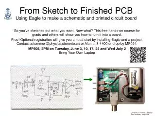
So you've sketched out what you want. Now what? This free hands-on course for grads and others will show you how to turn it into a board. Free! Optional registration will give you a head start by installing Eagle and a project. Contact astummer@physics.utoronto.ca or Alan at 8-4400 or drop by MP024. MP505, 2PM on Tuesday, June 3, 10, 17, 24 and Wed July 2 Bring Your Own Laptop From Sketch to Finished PCBUsing Eagle to make a schematic and printed circuit board University of Toronto – Physics Alan Stummer, May 2014
Course Overview • Assume some electronics knowledge • CAD: Computer Aided Design (poor name) • EDA: Electronic Design Automation (?) • Schematic capture then board layout (“CAD”) • Mentor, Cadence, Altium, Orcad, Kicad, Eagle • No file standards (except gerbers) • Some CADs can import from other vendors
The Process Schematic Capture Board Layout • Schematic capture • Board layout • CAM and BOM • Send out gerbers • Assemble and test CAM Libraries Board House BOM Order Parts PCB Assemble and Test
Schematic Capture Overview • Everything that is on the board, so someone else has everything necessary without you around • Only what is actually on the board, can add Notes for extra information • Symbols taken from library (libraries)
Board Layout Overview • Position components, add pours • Define rules if necessary • Manually or auto route • Clean up, add labels • DRC (Design Rule Checks)
CAM & Final Steps Overview • CAM converts the board into industry standard gerbers, simple and fast process • Send gerbers to board house • Make BOM, order parts • Get bare boards in few days • Assemble, test, finished!
Eaglewww.cadsoftusa.com • Schematic capture, PCB layout, CAM (no Spice) • For all but enterprise (no database connection) • Start with Control Panel (and global setups) • Select project, opens schematic and/or board
Schematic Capture 101 (where the circuit design happens) • Add components from library (more later) • Connect with wires • Modify, correct, repeat from 1, ad nauseam • Finish with ERCs
Schematic Commands Commands for adding components, changing parameters, connect with wires, move, group, delete, copy, attributes, polygons, ERC, name, value, get/change info, add text or lines, etc. • Case insensitive, only need first three letters • Five ways to execute a command: • Type command, e.g. mov(e) and Enter. • Hit function key, e.g. F7 if setup script was run • Select command from menu, e.g. Edit – Move • Click command icon, e.g. Move icon • Click command text, e.g. Move text
Start of Second ClassHands on – Fire up your laptops • Zooming • Move a component • Delete and add a net • Frames and title blocks • Layers
Zoom in Eagle Like riding a bicycle, zooming in and out takes practice. Annoying at first but get over it. • Use the mouse wheel • The zoom happens at the cursor • Wheel back to zoom out • Wheel ahead to zoom in
Move a Component • Select Move command: - hit F7 (if setup script was run) - type mov or move - click Move icon - click Move in command list - select Move from Edit menu • Left click on component (if a four-way arrow appears, Eagle does not know which object you are clicking so use right button to cycle through choices then left click) • Drag and drop component
Delete and Add a Net • Type delete or hit Backspace. • Left click on the net – gone! • To add a wire, type net or hit F5 • Left click at one connection point • Move cursor diagonally. Right clicks to see routing choices. By convention, use orthagonal only. • Click net through to other connection, click to end • To end at other than a valid connection, double click
Frames and Title Blocks Always add a frame with a title block. Other people will look at your work and need to know what it is. Fill in the title block with schematic name, dates, who did it and revision. Add revisions after the circuit changes. That is how others know what is the latest and what changed.
Layers • A layer is a category of information such as symbols, names, values, nets, buses, pins, info, guide and custom layers • Refer to a layer by name or number • To change which layers are visible, click icon • Can use display command, e.g. dis cab 96 -93, meaning display the Cabinet (custom layer 102) and Values layer (layer 96) but hide Pins (layer 93) • In Schematic show all but pins • Show specific layers only: dis none wir sym
ERCs Electrical Rule Checks are done in all CAD programs, just different formats. ERCs check for warnings and errors such as a net with inputs only, a net with two outputs, parts with no values, unconnected pins, etc. Can Approve warnings you wish to ignore. ERCs are run by erc command.
Scripts • Scripts are text files (with .scr extension) containing a series of commands. Edit with text editor. • Call explicitly (e.g. scr save) or from list of scripts by scr command • Example file exerpt: window fit write net
User Language Programs • A powerful programming language, similar to C, many proprietary constructs • Use existing ULPs or learn to write your own • Call explicitly (e.g. “run find”) or list of URLs by run • Example file excerpt: string showSch (int sht, int x, int y, string Targets, string Type) { string RunNext; sprintf (RunNext, "Grid mil; Edit .s%d; Window (%.66f %.66f); %s; Show @ %s\n\n", return RunNext; }
Good News - Eagle • Board and Library [windows] have the same feel as Schematic • All three use the same commands, layers, scripts and ULPs (when valid and applicable)
Board Layout 101(where the copper happens) • The components added to the schematic will be bunched in the corner • Place components • Route nets (manually and/or autorouter), move components and nets, repeat ad nauseam
Move a Component • Select move command (hint: move or F7) • Left click on component (if a four-way arrow appears, Eagle does not know which object you are clicking so use right button to cycle through choices then left click) • Drag and drop component • ...or hit Esc to cancel
Start of Third ClassFun [sic] with PCBs • What is a PCB? • Ripping up and adding nets • Dimension layer • Pours and power layers • Ground bounce • Bypassing • DRCs NB: - “Layers” can mean what is shown on the screen or the physical copper - On Board, nets are RIPped up, not DELeted
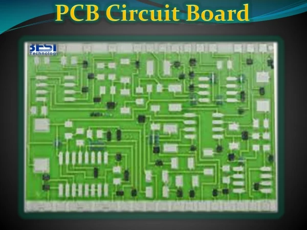
What is a PCB? • A FR4 substrate with copper layers both sides • FR4 is most common: woven fibreglass with resin, typically 1.58mm (0.062”) thick • Use Rogers 4350 for GHz - controlled permittivity but $$$ • Copper almost always “1oz”: 1oz of Cu per square foot, or 35μm. 2oz and more for high current - but $$$ • Usually 2-layer, can be 4, 6, 8, even 10. 2-layer is cheapest. >2 for BGAs, power planes. Example FR4 stackup 0.014"/0.028"/0.014" • Solder mask both sides, legend (“silk”) top only
Rip Up and Add a Net • Type ripup or hit F6 • Left click on a segment – gone! That segment is now unrouted (layer 19), in yellow • To rip a whole net, click on an unrouted segment • To route the net, type route or hit F5 • Left click near one end of the unrouted net. The net will start from the connection point • Move cursor. Cycle through right clicks to see routing choices. By convention, use 45° and 90° only • Route through to connection point, click to end • To end at other than a valid connection, double click
Grids • All layouts are to the current grid. Grids can be metric (mm), inch (in) or milli-inch (mil). For example: gri mm on 1(1mm grid, visible) gri 0.18(0.18 whatever in current scale and visibility) gri off(hide the grid) • If a component or net is not on the current grid, to snap it to the grid hold CTRL while clicking • Suggest: Schematic: 0.05” (1.27mm) or 0.1” (2.54mm) Board: 1mm (placement) and 0.36mm (routing)
Dimension Layer The dimension layer (20) defines the dimensions of the board. It must be continuous. The board house will cut the board to the dimension layer shape. One layout can have multiple boards with multiple dimension outlines. Dimension lines can be moved like any other lines. • If there are no dimensions, type wire • Select dimension layer, click on board corner • Click around the desired board outline
Groups • Two ways to select: • group or F8 then select rectangle with left button • group or F8 then left click around odd shaped area, end with right click to jump back to start point • Many commands will work on the group with a right click, e.g. move or delete • To copy a group, select group then hit CTRL-X and left click. To paste, command paste or CTRL-V then click and locate and click again
Pours Always fill layers with as much copper as possible. Components and nets will connect or cut into pours as needed. • Type command polygon • Left click at start, usually board corner • Like routing, click out the board, ending at the first corner • Type name then click the polygon edge and give it the net name, such as AGND or +5V • Type ratsnest or hit F4 to untangle the unrouted nets and to pour the pours
Ground Pour Effects Poor grounding Bad ground bounce Solid grounding Minimal ground bounce
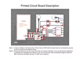
Sample Top Layer (of four) From T.I. MSP430 development kit – a watch
Bypassing Capacitors • Ceramic bypass caps must be as close as possible to the IC • Usually 0.1μF, NPO or X7R dielectric Bypass 15mm away Bypass 2mm away
DRC 101 The Design Rule Checks are industry standard, although the format differs with different CADs. The DRCs define layers (how many, what thickness), clearances (copper, space), distances (to dimension, between holes), drills (vias), thermals, mask (solder stop) and a few odds and ends. Use a predefined DRC file. Industry standard net and space are 0.18mm or 0.007”, although can do down to 0.13mm.
Class #4 • Board and Schematic linking • Autorouter • Library (libraries) • Adding a complete component • ERC and DRC again • CAM
Schematic and Board Are Linked Schematic and Board forward and back annotate. Never, ever, close Board or Schematic and then make changes! ...unless you know what you are doing. Out of sync schematic and board can be fixed. Use erc command for list of discrepancies.
Autorouter 101 Not included with Freeagle (free Eagle). Industry standard, although varies in format. Define the rules then let the computer route everything. Does a reasonable job, have to manually route nets autorouter could not do. Use a predefined autorouter file.
Library 101 The library (or libraries) contain the symbol for the schematic and the package(AKA decal or footprint) for the board, combined into a device. All components are taken from the library. • Draw the symbol. Add and name pins. Add >NAME to name layer (95) and >VALUE to value layer (96). • Draw the package. Add and name pads, add place (layer 21) for outline, add >NAME to name layer. • In device, add the only symbol and ref des prefix (e.g. R, C). Add package(s), connect pins to pads. • Be sure to update library in Schematic or Board to implement any changes.
Create a Component74HCT86 Quad XORhttp://www.diodes.com/datasheets/74HCT86.pdf • Create a single XOR gate • Copy it for four gates (for fixed symbols) • Create the TSSOP-14 package (if necessary) • Create a quad XOR device • Add the symbol(s) and package • Associate the pins and pads
Add a Component • In Schematic, type add or F6 • Select the device and package • Click on schematic to drop it on • Use move or F7 to move it • Use net or F5 to connect • In Board, move the decal and route
ERC and DRC Nearing the end. When the board seems complete, run all checks again. ERCs (type erc) should be okay if done before and no changes were done to the schematic. Type drc in Board. Open a predefined DRC file. Click Select. It will spit out all of the issues. Either fix them or approve them. Command dcr; will run last DRC checks again.
CAM Computer Aided Manufacturing turns the proprietary Eagle format board into an industry standard gerber file. • Open the CAM processor • Open a predefined CAM job file • Click on Process Job • Common problem is undefined drills. Open the drill file in an ASCII editor, add required drills. Process job again
Gerbers and NC Drill Gerbers are the industry standard ASCII files defining the board. CAM generates one gerber file for each layer. They are long and tedious and cryptic to read, don't bother. The generated NC drill file defines the drills. To view gerbers, use Viewmate or similar instead of the same program which made the gerbers.
Getting the Board Made • Run the BOM (Bill Of Materials), order parts first to be sure all is available • Send the files to the PCB manufacturer • Boards usually made in even numbers only • Usually about a week, <$200 for 80x100mm pair of boards, delivered with tax. Can save cost by not having solder mask and silk screen, but beware of bare copper • PCB manufacturers offer electrical testing, often do assembly up to full testing
PCB ManufacturersAKA Board houses or Fabs PCBs fail – all board houses are not equal Standard is 0.062” (1.6mm) FR4 with 1oz copper, 2‑layer most common for our work • Alberta Printed Circuits (apc.com), Canadian, very reliable, fast, good price, flexible requirements, 0.007” (180μ) track and space, 0.017” (430μ) vias, FR4 and Rogers 4350 • Pentalogix (pentalogix.com), US or offshore, okay price but watch for shipping and duties, less flexible, 5mil track & space, 8mil via • Dirt Cheap Dirty Boards (dirtypcbs.com), China, cheap, slow, fixed sizes, fixed quantities, 2-layer only, 5mil t&s, 12mil via • Imagineering (pcbnet.com), US, $25/$50 intro offer only
Build and Test Finally, assemble and test the board. Use a microscope or magnifier, tweezers, smoke eater or good ventilation, 0.5mm soldering tip for small parts, larger for others, 0.5mm solder with water clean flux. Wash under tap, dry with air. Assemble in stages, start with power supplies. Build up section by section. Spin the board if too many white wires or fixes.
Class #5 • More Eagle commands • Grounding in a nutshell • Transmission lines • Common IC and passive packages • Back to Libraries
More Eagle Commands • SHOw a part, e.g. sho r1 or sho n$10 • INFo, general info on that object • MARk, a spatial reference point • NAMe a part • VALue, give value, e.g. LM3478MB or 10K • TEXt, add free text, e.g. tex Notes: 1)Lorem ipsum • WIRe, a non-conducting line • CIRcle, ARC, a circle or part of a circle.
INVoke, add another gate • ATTributes, further component descriptions such as manufacturer or specific part number • CHAnge: [text] alignment, cap, class, display, font [type], layer, width, [line] style, package, [font] ratio, [font,drill] size, thermals, orphans, isolate, text • BUS, a way to show any grouped nets • SPLit, break any line • SMAsh, allow attributes of part to be loose • VIA, add an explicit via to a net or pour
HOLe, a non-conducting hole (drill) • RIPup;, semi-colon means rip everything • LOCk, lock part or group from moving • RANk, the hierarchy of overlapping polygons, such as a tab in a pour, 1 (highest) to 7 • SET Option.ToggleCtrlForGroupSelectionAndContextMenu 1; Remember, any command can also go in a script or assigned to a key combination (Options – Assign). Get help by entering command then F1.
The Evils of Grounding This is the single biggest cause of failure of a layout. No ground is perfect. Treat all copper as a series of resistors and inductors. Always look where current is going, especially when mixing analog with digital or switching. Split ground planes to isolate currents.
Transmission Lines • Rule of thumb: use a transmission line if net is longer than 0.1λ or is not very straight. e.g. necessary harmonics are up to 300MHz then can have up to about 6cm nets without a transmission line • Microstrip: a transmission line on an outer layer • Stripline: a buried transmission line (>2 layers) • FYI, on 0.062” FR4, need 3.5mm wide net with ground plane on other side for 50Ω • Use an online PCB impedance calculator