Download
1 / 15
160 likes | 476 Vues
Andreev Reflection in Quantum Hall Effect Regime. H. Takayanagi 髙柳 英明. Tokyo University of Science,Tokyo International Center for Materials NanoArchitechtonics (MANA), National Institute for Materials Science, Tsukuba.

E N D
Andreev Reflection in Quantum Hall Effect Regime H. Takayanagi髙柳 英明 Tokyo University of Science,Tokyo International Center for Materials NanoArchitechtonics (MANA), National Institute for Materials Science, Tsukuba
Superconducting Junctions using AlGaAs/GaAs Heterostructures with High Hc2 NbN Electrodes Hideaki Takayanagi, Tatsushi Akazaki & Yuichi Harada , NTT Basic Research Laboratories Minoru Kawamura, Riken Junsaku Nitta, Tohoku University
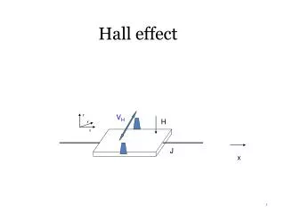
Andreev Reflection An incident electron from the normal conductor is reflected as ahole and aCooper pair is created in the superconductor. The differential resistance of the S/N interface decreases or increases within the superconducting energy gap depending on the Andreev reflection probability (A) and normal reflection probability (B).
Andreev Reflection in High Magnetic Field • A 2DEG exhibits QHE in a strong perpendicular magnetic field. The QHE is represented in terms of edge states. • Andreev reflection between superconductor and edge states was first proposed by Zyuzin[1] and have been investigated theoretically and experimentally by several authors. [1] A. Yu Zyuzin Phys. Rev. B 50(1994) 323. [2] H. Takayanagi and T. Akazaki, Physica B 249-251(1998)462. [3] T. D. Moore and D. A. Williams, Phys. Rev. B 59(1999)7308.
Sample SNS junction withNbN sueprconducting electrodes&a 2DEG in a AlGaA/GaAs single heterostructure • Advantages of these materials • NbN • High Hc2 > 18T • 2DEG in AlGaAs/GaAs heterostructure • High electron mobility • Low carrier density • Problem • High Schottky barrier between NbN and GaAs
Sample Fabrication AuGeNi layer is inserted between NbN and GaAs. The samples are annealed at 450℃ in N2 atmosphere.
Properties of 2DEG &NbN n=7.36x10¹⁵m-2 m=18.3m2/Vs Magnetic field dependence of a Hall-bar shaped sample with normal conductor electrode (left). Temperature dependence of the resistance of NbN thin film (right).
V Dependence of dV/dI The differential resistance of a SNS junction. A decrease of a resistance (about 6%) is observed within V ~ 5mV, which corresponds to 2D. D is the superconducting energy gap of NbN.
Magnetic Field Dependence I dV/dI v.s. V curves at weak magnetic fields.As magnetic field is increased, the Hall voltage arises in the 2DEG. So the voltage drop mainly occurs in the 2DEG rather than S/N interface. This causes the energy gap structure moves to higher voltages.
Magnetic Field Dependence II Magnetic field dependence of zero-bias resistance. The inset shows the junction length L dependence of DR.
Remarkable Features • The SNS junctions with superconducting electrodes show deep resistance minima between n=4 and n=3. • The minima does not appear in the junction with normal electrode. • The resistance minima become smaller as the junction length L become longer. • Resistance of the SNS junctions are almost same as the usual value h/ne2, when the filling factor n is integer. • These resistance minima can be explained byAndreev reflection.
A Simple Explanation Imported from a model of S/N junctions at zero magnetic field. (1)
L-dependence The transmission probability T is calculated using Eq.(1) for several samples with different junction length L. T is almost proportional to 1/L as same as diffusive case.
Summary • The SNS junction using a 2DEG in an AlGaAs/GaAs single heterostructure and High Hc2 superconductor NbN was fabricated. • The transport properties of the SNS junctions have been investigated in the quantum Hall regime. • Large resistance minima appear between the quantum Hall plateau, which are explained in terms of Andreev reflectionbetweenNbNand extended states at the center of the Landau level.