Download
1 / 23
240 likes | 496 Vues
Technology and Historical Perspective: A peek of the microprocessor Evolution. Moore’s Law and Headcount. Along with the number of transistors, the effort and headcount required to design a microprocessor has grown exponentially. Intel 486™ DX CPU. Design 1986 – 1989 25 MHz, 33 MHz

E N D
Technology and Historical Perspective:A peek of the microprocessor Evolution \CPEG323-08F\Topic1a.ppt
Moore’s Law and Headcount • Along with the number of transistors, the effort and headcount required to design a microprocessor has grown exponentially \CPEG323-08F\Topic1a.ppt
Intel 486™ DX CPU • Design 1986 – 1989 • 25 MHz, 33 MHz • 1.2 M transistors • 1.0 micron • 5 stage pipeline • Unified 8 KByte code/data cache (write-through) • First IA-32 processor capable of executing 1 instruction per clock cycle \CPEG323-08F\Topic1a.ppt
Pentium® Processor • Design 1989 – 1993 • 60 MHz, 66 MHz • 3.1 M transistors • 0.8 micron • 5 stage pipeline • 8 KByte instruction and 8 KByte data caches (writeback) • Branch predictor • Pipelined floating point • First superscalar IA-32: capable of executing 2 instructions per clock \CPEG323-08F\Topic1a.ppt
Pentium® II Processor • Design 1995 – 1997 • 233 MHz, 266 MHz, 300 MHz • 7.5 M transistors • 0.35 micron • 16 KByte L1I, 16 KByte L1D, 512 KByte off-die L2 • First compaction of P6 microarchitecture \CPEG323-08F\Topic1a.ppt
Pentium® III Processor (Katmai) • Introduced: 1999 • 450 MHz, 500 MHz, 533 MHz, 600MHz • 9.5 M transistors • 0.25 micron • 16 KByte L1I, 16 KByte L1D, 512 KByte off-chip L2 • Addition of SSE instructions. SSE: Intel Streaming SIMD Extensions to the x86 ISA \CPEG323-08F\Topic1a.ppt
Pentium® III Processor (Coppermine) • Introduced: 1999 • 500MHz … 1133MHz • 28 M transistors • 0.18 micron • 16 KByte L1I, 16 KByte L1D, 256KByte on-chip L2 • Integrate L2 cache on chip, It topped out at 1GHz. \CPEG323-08F\Topic1a.ppt
Pentium® IV Processor • Introduced: 2000 • 1.3GHz … 2GHz … 3.4GHz • 42M … 55M … 125 M transistors • 0.18 … 0.13 … 0.09 micron • Latest one: 16 KByte L1I, 16 KByte L1D, 1M on-chip L2 • Very high clock speed and SSE performance \CPEG323-08F\Topic1a.ppt
Intel® Itanium® Processor • Design 1993 – 2000 • 733 MHz, 800 MHz • 25 M transistors • 0.18 micron • 3 levels of cache • 16 KByte L1I, 16 KByte L1D • 96 KByte L2 • 4 MByte off-die L3 • VLIW, degree 6, in-order machine • First implementation of 64-bit Itanium architecture \CPEG323-08F\Topic1a.ppt
Intel® Itanium 2® Processor • Introduced: 2002 • 1GHz • 221 M transistors • 0.18 micron • 3 levels of cache • 32 KByte I&D L1 • 256 KByte L2 • integrated 1.5MByte L3 • Based on EPIC architecture • Enhanced Machine Check Architecture (MCA) with extensive Error Correcting Code (ECC) \CPEG323-08F\Topic1a.ppt
Cache Size Becoming Larger and Larger 2002: Itanium-2 1993: Pentium 1997: Pentium-II Level 1: 16K KByte I-cache, 16 KByte D-cache Level 2: 256 KB Level 3: integrated 3 MB or 1.5 MB • 8 KByte I-cache and 8 KByte D-cache 16 KByte L1-I, 16 KByte L1-D 512 KByte off-die L2 \CPEG323-08F\Topic1a.ppt
Motorola’s PowerPC 604 Pentium \CPEG323-08F\Topic1a.ppt
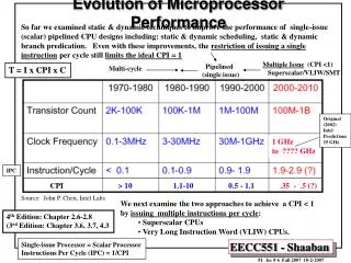
Technology Progress Overview • Processor speed improvement: 2x per year (since 85). 100x in last decade. • DRAM Memory Capacity: 2x in 2 years (since 96). 64x in last decade. • DISK capacity: 2x per year (since 97). 250x in last decade. \CPEG323-08F\Topic1a.ppt
Data source: http://www.spec.org/cpu2000/results/cint2000.html http://www.geek.com/procspec/procspec.htm http://www.bayarea.net/~kins/AboutMe/CPUs.html Main observation: application of additional resources yields diminishing return in performance In addition: - heat problem - design complexity \CPEG323-08F\Topic1a.ppt
Pentium M Thermal Maps from the Pentium M obtained from simulated power density (left) and IREM measurement (right). Heat levels goes from black (lowest), red, orange, yellow and white (highest) Figures courtesy of Dani Genossar and Nachum Shamir in their paper Intel ® Pentium ® M Processor Power Estimation, Bugdeting, Optimization and Validation published in the Intel Technical Journal, May 21, 2003 \CPEG323-08F\Topic1a.ppt
What Is Next ? • Move to “multiprocessor on a chip” ? • cooler • simpler • cheaper • … \CPEG323-08F\Topic1a.ppt
Alternatives: Multi-Core-On-A-Chip • Driven by technology reality (too hot and too complex) • Examples: • Intel multi-core roadmap (see EE Times) • AMD Opteron • Outcomes from HPCS projects from DARPA • IBM Multi-Core Chips: • The CELL product - IBM, Sony, Toshiba • IBM/ETI Cyclops Product • Others (e.g. Clearspeed, etc.) • Box vendors are beginning adapting multi-core chips \CPEG323-08F\Topic1a.ppt
IBM Power6 Multicore Chip • Uses 65 nm technology with 790 million transistors running at 3.5, 4.2 and 4.7 GHz • However IBM claims to have 6GHz prototypes • Up to 8 instructions fetch (8-way Superscalar) • Dual Processor Core • Each Core Capable of two logical threads (SMT) • 4 MB Private L2 Cache per processor • 32 MB L3 Shared Cache • Butterfly Physical Layout for L2 caches • Reduced physical distance to the L1 data caches inside the cores • Doubles the physical width of the data bus Courtesy of Le, H. Q., et. Al. “IBM POWER6 Micro-architecture”, IBM 2007 \CPEG323-08F\Topic1a.ppt
Quad AMD “Barcelona” OpteronTM • Created using 65 nm technology using SOI • Four Processor Cores • 512 Private L2 Cache per processor • 2 MB Shared L3 Cache • Frequencies ranging from 2 to 1.8 GHz per core • Enhanced PowerNow!TM and CoolCoreTM Technologies • Support HyperTransport 3.0 • 8 point to point per socket \CPEG323-08F\Topic1a.ppt
ClearSpeed CSX700 • 10 W Average power dissipation • 33 GFLOPS sustained double precision DGEMM • 96 Gbytes / s internal memory • 3.2 Gbytes / s external memory • 2 x 3.2 Gbytes / s inter chip bandwidth • 192 high-performance processing elements, each with dedicated memory • 6 Kbytes high bandwidth memory per processing element • 128 Kbytes on-chip scratchpad memory • 64-bit DDR2 DRAM interface with ECC support • ClearConnect NoC provides on-chip and inter-chip data network • Host interface and debug port • 64-bit virtual, 48-bit physical addressing • On-chip instruction and data caches • On-chip DMA controller Courtesy of CSX700 Overview on http://www.clearspeed.com/ \CPEG323-08F\Topic1a.ppt
IBM Cyclops-64 Chip Architecture On-chip bisection BW = 0.38 TB/s, total BW to 6 neighbours = 48GB/sec \CPEG323-08F\Topic1a.ppt