Design Rules
Design Rules. EE213 VLSI Design. Stick Diagrams. VLSI design aims to translate circuit concepts onto silicon stick diagrams are a means of capturing topography and layer information - simple diagrams Stick diagrams convey layer information through colour codes (or monochrome encoding

Design Rules
E N D
Presentation Transcript
Design Rules EE213 VLSI Design
Stick Diagrams • VLSI design aims to translate circuit concepts onto silicon • stick diagrams are a means of capturing topography and layer information - simple diagrams • Stick diagrams convey layer information through colour codes (or monochrome encoding • Used by CAD packages, including Microwind
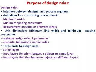
Design Rules • Allow translation of circuits (usually in stick diagram or symbolic form) into actual geometry in silicon • Interface between circuit designer and fabrication engineer • Compromise • designer - tighter, smaller • fabricator - controllable, reproducable
Lambda Based Design Rules • Design rules based on single parameter, λ • Simple for the designer • Wide acceptance • Provide feature size independent way of setting out mask • If design rules are obeyed, masks will produce working circuits • Minimum feature size is defined as 2 λ • Used to preserve topological features on a chip • Prevents shorting, opens, contacts from slipping out of area to be contacted
Design Rules - The Reality • Manufacturing processes have inherent limitations in accuracy and repeatability • Design rules specify geometry of masks that provide reasonable yield • Design rules are determined by experience
Problems - Manufacturing • Photoresist shrinking / tearing • Variations in material deposition • Variations in temperature • Variations in oxide thickness • Impurities • Variations between lots • Variations across the wafer
Problems - Manufacturing • Variations in threshold voltage • oxide thickness • ion implantation • poly variations • Diffusion - changes in doping (variation in R, C) • Poly, metal variations in height and width -> variation in R, C • Shorts and opens • Via may not be cut all the way through • Undersize via has too much resistance • Oversize via may short
Meta Design Rules • Basic reasons for design rules • Rules that generate design rules • Under worst case misalignment and maximum edge movement of any feature, no serious performance degradation should occur
Advantages of Generalised Design Rules • Ease of learning because they are scalablem portable, durable • Longlevity of designs that are simple, abstract and minimal clutter • Increased designer efficiency • Automatic translation to final layout
References • Pucknell and Eshraghian pages 62 - 92 • Fabricius pages76 - 82