Purpose of design rules: Design Rules • Interface between designer and process engineer
300 likes | 686 Vues
Purpose of design rules: Design Rules • Interface between designer and process engineer • Guidelines for constructing process masks – Minimum width – Minimum spacing constraints – Requirement on same or different layers

Purpose of design rules: Design Rules • Interface between designer and process engineer
E N D
Presentation Transcript
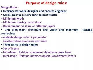
Purpose of design rules: Design Rules • Interface between designer and process engineer • Guidelines for constructing process masks – Minimum width – Minimum spacing constraints – Requirement on same or different layers • Unit dimension: Minimum line width and minimum spacing constraints – scalable design rules: λ parameter – absolute dimensions: micron rules • Three parts to design rules: – Set of layers – Intra-layer: Relations between objects on same layer – Inter-layer: Relation between objects on different layers
The design rules are usually described in two ways: Micron rules, in which the layout constraints such as minimum feature sizes and minimum allowable feature separations are stated in terms of absolute dimensions in micrometers, or, (ii) Lambda rules, which specify the layout constraints in terms of a single parameter () and thus allow linear, proportional scaling of all geometrical constraints.
Stick diagram: It is useful for planning the layout and routing of integrated circuits. In a stick diagram, every line of a conducting material layer is represented by a line of a distinct color. Here we will use the basic color coding below: The width of a line is not important, as stick diagrams give only wiring and routing information
A stick diagram is thus a schematic representation of a circuit at the physical design level. With a little practice, you will be able to read a stick diagram and translate it into a conventional circuit schematic. In the early days of MOS integrated circuits it was noticed that when a chip was illuminated with a white light source, each conducting layer had a distinct coloring associated with it when viewed under a microscope
A pFET is described by the same "red over green" coding, but the crossing point is contained within an nWell boundary
poly (red) cannot contact n-diffusion (green) and p-diffusion (yellow).
when we want to connect poly (red) to n-diff (green) or p-diff (yellow), we must first connect poly (red) to metal1 (blue) and then metal1 (blue) to n-diffusion (green) or p-diffusion (yellow) Metal1 (blue) can contact n-diffusion (green), p-diffusion (yellow) and poly (red), but remember contact is needed, otherwise no connection is made, even if the layers are crossed Wrong connection
Basic Rules for constructing stick diagram The rules for constructing stick diagrams are based on the characteristics of the conducting layers • Only the routing is important, not the line widths
Conclusion: Stick diagrams provide an easy approach to performing simple CMOS circuit layouts. Planning a physical design using stick diagrams before going to a CAD tool can save a lot of time and energy.
CMOS Inverter Stick diagram Step-1:Two horizontal wires are used for connection with VSS and VDD. This is done in metal2, but you can decide to use metal1 instead.
Step-3: Then the gates of the transistors are joined with a polysilicon wire, and connected to the input.
Step -4:The drains of two transistors are then connected with metal1 and joined to the output. There cannot be direct connection from n-transistor to p-transistors
Step-5: The sources of the transistors are next connected to VSS and VDD with metal1. Notice that vias are used, not contacts. Fig: Stick diagram of CMOS Inverter
Stick diagram continued------- NAND2 gate NAND2 gate Stick diagram
Sketch the stick diagram of the expression given below Fig: Stick diagram of the above expression
Minimum dimensions and spacings (using λ-rules) Note that λ=1/2