Download
1 / 11
110 likes | 273 Vues
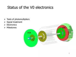
V0C. V0A. Status of the V0 electronics. Tests of photomultipliers Signal treatment Electronics Milestones. Photo-multiplier. 16. 19. 16. 19. 15. Charge, gain, time resolution. Signal x 10 + 25 m cable. Signal amplitude. 75 mV – 1.5 V. ( 125 mV – 1.5 V). Signal amplitude.

E N D
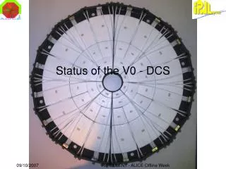
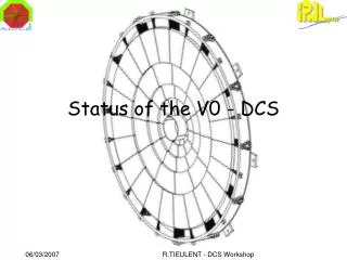
V0C V0A Status of the V0 electronics • Tests of photomultipliers • Signal treatment • Electronics • Milestones
16 19 16 19 15 Charge, gain, time resolution Signal x 10 + 25 m cable
Signal amplitude 75 mV – 1.5 V (125 mV – 1.5 V) Signal amplitude 15 mV – 300 mV Signal charge Signal charge 15 pC - ~2500 pC 15 pC - ~2500 pC (25 mV – 300 mV) Signal amplitude (25 pC - ~2500 pC) (25 pC - ~2500 pC) 3 mV – 3 V (5 mV – 5 V) To TRD wake-up G=5 50 ohms To V0 FEE threshold disri. G=5 G=5 50 ohms OR NINO shaper (0.1 – 2 pC) 2 ns Anode PM signal To V0 FEE QDC G=1 50 ohms Signal amplitude Signal charge 3 mV – 3 V 0.6 pC - 600 pC (5 mV – 5 V) (1 pC - 1000 pC) Pulse treatment
data from V0C buffer X 4 HPTDC (8 ch/chip) L1 buff data from V0A DAQ data time hit L2 individual offset THR charge L0 compensation buffer V0A 1 sum for + 4 NINO + + BBA (BBC) BB MB triggers each ring x 32 anodes 11 (3) - + buffer 1 sum for 4 BGA(BBC) BBA (BGC) + + - NINO each ring BG MB triggers adjustable windows adjustable windows (step of 20ps, range of 10 ns) (.5 to 12ns, step of .5ns) BGA BGC THRmult. multiplicity triggers (V0C) buffer from V0C ADC from V0C 4 4 5 triggers, eg : 4 1 sum for - minimum bias + 4 - beam/gaz (right) FPGA each ring buffer - beam/gaz (left) THRcharge 4 - centrality ADC - multiplicity BC programmable programmable centrality triggers thresholds from V0C integration gate width (from 3ns to 36ns, step of 3ns) FEE
C A A C C A Timing for BB and BG
V0A THR -11 ns buffer 1 sum for 4 l t NINO BGA + each ring x 32 anodes buffer 1 sum for 4 BBA + NINO each ring +11 ns adjustable windows adjustable windows (step of 20ps, range of 10 ns) (.5 to 12ns, step of .5ns) BGA -3 ns A BGC BGC & + BB C BBC + +3 ns V0C Minimum-bias triggers • Starting from the discriminator or the NINO signal • BB signal detected in time windows centered at +11 ns (V0A) and +3 ns (V0C) • BGAsignal detected in time windows centered at -11 ns (V0A) and +3 ns (V0C) • BGC signal detected in time windows centered at +11 ns (V0A) and -3 ns (V0C) bbc bba
V0 mechanics milestones • Fall 2004: • End 2004: • March 2005: sector ‘0’ of V0A (Mexico) and V0C (Lyon) PRR submission • Fall 2005: V0C ready for commissioning,… PMT characterization (Lyon) (MIP from each channel,… noise, gain of each PMT) • End 2005: V0A ready for commissioning,… PMT characterization (Mexico) (MIP from each channel,… noise, gain of each PMT) • Spring 2006: • June 2006: V0C ready for installation in ALICE (array + fibre bundles + PMT mechanics) • End 2006: V0A ready for installation in ALICE (array + fibre bundles + PMT mechanics) • Responsibles: Mechanics: J.Y. Grossiord (Lyon), XXXX (Mexico)
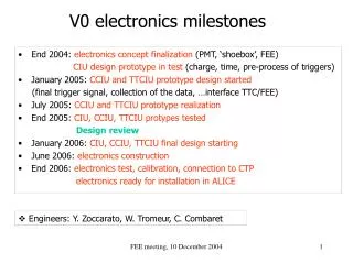
V0 electronics milestones • Fall 2004: electronics concept finalization • End 2004: CIU design prototype test (charge, time, pre-process of triggers) • March 2005: • Fall 2005: (final trigger signal, collection of the data, …interface TTC/FEE) CCIU and TTCIU design prototype test PRR submission • End 2005: CIU, CCIU, TTCIU electronic design, setting • Spring 2006: electronics design ready for realization • June 2006: electronics construction • End 2006: electronics test, calibration electronics ready for installation in ALICE • Responsibles: Electronics: Y. Zoccarato
V0 milestones • Fall 2004: electronics concept finalization • End 2004: CIU design prototype test • March 2005: sector ‘0’ of V0A (Mexico) and V0C (Lyon) PRR submission • Fall 2005: V0C ready for commissioning, PMT characterisation (Lyon) CCIU and TTCIU design prototype test PRR submission • End 2005: V0A ready for commissioning (Mexico) CIU, CCIU, TTCIU electronical scheme • Spring 2006: electronics design ready for realization • June 2006: V0C ready for installation in ALICE electronics construction • End 2006: V0A ready for installation in ALICE electronics test, calibration electronics ready for installation in ALICE • Responsibles: Electronics: Y. Zoccarato Mechanics: J.Y. Grossiord (Lyon), XXXX (Mexico)