Download
1 / 9
90 likes | 206 Vues
On May 26, 2009, Mauro Citterio led a meeting to discuss the progress of LAr electronics, focusing on integrating readout architectures and system components. The working group's priorities include addressing data flow in front-end electronics and coordinating designs for preamps and optical links. Various institutions, including BNL and Nevis, shared updates on their R&D efforts. The meeting emphasized the need for collaboration, reviewing power supply architectures, and establishing testable designs amidst the challenges posed by radiation environments. ###

E N D
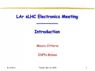
LAr sLHC Electronics Meeting________Introduction Mauro Citterio INFN Milano Tuesday, May, 26, 2009
A new meeting ..... how nice !! • To inform people about the “foreseen LAr electronics” • the “readout architecture system integration” working group it is slowly starting to operate (bi-weekly phone meetings) • various components need to be “revisited” • Front-end boards • HEC preamps • “Other” boards • Optical data Transmission • Interface to TTC • ROD/back end • L1/TDAQ Interface • PS System (including HEC specific PS) • Ctlr., Cfg. and Monitoring • Interface to other subsystems • the various issues need to be addressed following a hierarchy • To progress toward an ATLAS LoI • an index of arguments to be included in the “calorimeter chapter” of the letter • due by May 2009 Tuesday, May, 26, 2009
What has been discussed so far ..... • Highest priority has been given, up to now, to the “data flow” in the front-end electronics • Activities were initiated spontaneously at various institutions and needed to be “coordinated” • BNL/PENN Design in IBM SiGe technology of preamp and shaper) (* Milano and Orsay also part of the SiGe R&D) • Nevis Design in IBM RF8 CMOS technology of a fast ADC + system aspects (Gustaaf presentation) • SMU Design in SOS of Link on Chip (LOC) + participation to the Cern VERSATILE common project (Jingbo presentation) • MPI Design of HEC preamps (technology to be chosen) • Avoid that “designs and ideas” grow isolated • Included IMMEDIATELY in the design the needs of the PS system Tuesday, May, 26, 2009
Common designs ? • Optical link • We need to pursue the SMU design (LOC) • Design is well advanced and close to our requirements • We need to present to CERN our necessities • The CERN GBT design does not satisfy our requirements • A LAr set of specifications is under preparation and it is going to be presented soon to Philippe Farthoutto verify if a FUTURE generation of GBT could satisfy our needs (included in Jingbo presentation) • We need to explore the “commercial world” • Work is on stand-by not enough manpower • ADC • Again we need to pursue our own design (Nevis) • No solution available • Even if the commercial world has done a lot in this field • CERN is still thinking to a “common project” Stay connected Tuesday, May, 26, 2009
How the PS system will evolve ?? • A review of the present solution is mandatory • to identify the weak points • For the future .. • avoid the “proliferation” and “anarchy” of the voltage levels • adopt solutions that will benefit from the industrial mainstream • Perform a detailed failure analysis • Design with testability in mind • Part of the phone meetings will include thoroughly discussion on this item • PS for BARREL and END-CAPs BUT ALSO • PS for the HEC Tuesday, May, 26, 2009
The PS present solution 19 voltage regulators/FEB Centralized architecture Tuesday, May, 26, 2009
Strategy for a Rad-Tolerant LVPS R&D Tuesday, May, 26, 2009 • Radiation environment assumed to scale x10 • Total power budget of electronics assumed to remain the same • Reduce the number and levels of the voltages • Use of point of load “converters/regulators” (Chen presentation) • Possibility of adopting new topologies in the Main Converter • Reduced voltage across devices • Optimized design of magnetics • Higher switching frequency • Design a Single Failure Tolerant System • Migration of the LVPS Architecture • Distributed Power Architecture • A main converter generates a distribution bus and on-boards point-of-load (POL) converters directly supply low voltages to loads • Intermediate Bus Architecture • In addition to the generation of a main voltage bus, as in the DPA but typically higher,a second set of bus voltages is provided, then lower voltages are given by the POL converters
Possible Architecture Solution Card #3 Card #2 Card #1 Card #2 POL Converter niPOL Converter niPOL Converter POL Converter niPOL Converter POL Converter niPOL Converter niPOL Converter LDO POL Converter LDO POL Converter LDO niPOL Converter POL POL POL POL POL POL POL POL POL POL POL POL POL POL POL Distributed Power Architecture 280 VDC V1x VDC Crate Card #1 Main Converter V2x VDC (ex- LVPS) Intermediate Bus Architecture Tuesday, May, 26, 2009
Other activities in progress ..... • Some ROD/Back-end progresses have been made • Mostly by the same persons active in the front-end • BNL (Chen presentation) • It’s time to open the discussion to other groups • A mailing list is extracted by the “old BESG organization” • Significant amount of new ideas to be discussed • Interface to other subsystem should be addressed • How to get organized • Have all interested people join the bi-weekly phone meeting • The proposed day and time is FRIDAY 3:00 PM (CERN time) • Intensify the discussion if necessary • Report at the next LAr week Still many discussion and goals to be achieved … let’s start Tuesday, May, 26, 2009