Download
1 / 52
530 likes | 790 Vues
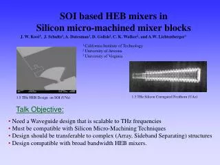
SOI based HEB mixers in Silicon micro-machined mixer blocks. J. W. Kooi 1 , J. Schultz 3 , A. Datesman 3 , D. Golish 2 , C. K. Walker 2 , and A.W. Lichtenberger 3. 1 California Institute of Technology 2 University of Arizona 3 University of Virginia.

E N D
SOI based HEB mixers in Silicon micro-machined mixer blocks J. W. Kooi1, J. Schultz3, A. Datesman3, D. Golish2, C. K. Walker2, and A.W. Lichtenberger3 1 California Institute of Technology 2 University of Arizona 3 University of Virginia 1.5 THz Silicon Corrugated Feedhorn (UAz) 1.5 THz HEB Design on SOI (UVa) Talk Objective: • Need a Waveguide design that is scalable to THz frequencies • Must be compatible with Silicon Micro-Machining Techniques • Design should be transferable to complex (Array, Sideband Separating) structures • Design compatible with broad bandwidth HEB mixers.
Waveguide vs. Open Structure Advantages: Advantages: • Beam well defined (f/D and waist, astigmatism) • Simple assembly • Rapid prototyping • Extendable to more complicated structures • Inexpensive Disadvantages: Disadvantages: • Beam not too well defined • Lot of Engineering time, i.e. expensive • Difficult to extend beyond single pixel
Lester and Benford et. al Spectral cooling lines of collapsing clouds in star forming regions. Science Objectives: Cooling of Interstellar and Circum Stellar Dust Continuum vs. Line Radiation • Turbulence in the ISM, • Structure of clouds, • Spatial studies of clouds (mapping, spectral imaging) • Line surveys of a wide range of molecular and atomic species. • Distant and possibly prime-evil galaxies. Z=1-5,
Line Sources Atmospheric Astrophysics - Point Sources: Red Shift Confirmation (SCUBA, SHARCII, BOLOCAM…) Extra Galactic Molecular Species Turbulence in the ISM Probing Star Forming Regions - Pressure broadened lines - Strong lines - Atmospheric noise -Extended Sources (Clouds) - Large IF bandwidth (10 GHz +) Spectral Line Surveys - Sideband Separating Spatial studies of clouds (spectral mapping) Large IF bandwidth (8 GHz+) Instrumentation: Instrumentation: - Sideband separating mixers - Stable Receivers (Balanced – LO noise Cancellation) • Double Sideband Mixers • (Open Structure or Wg) - Deep Integrations (Correlation mixers) - High Sensitivity (Sideband Separating/Array Rx) - Build image by scanning platform - Automated spectral line surveys (Balanced mixers)
Balanced Mixer Configuration • - Separate LO Port Much lower LO requirement • over traditional DSB and SSB designs. • Reduced (11-15 dB) Local Oscillator Amplitude Noise • Improved Stability and increased Sensitivity • Easy to automate over large RF Bandwidth • (spectral line surveys)\
Correlation Mixer Configuration -Two Pixels; (On Source - Off Source), Improved Sky Subtraction -Deep integrations for Extra Galactic (High z) spectral line work. Specifications: • 100mK (100 MHz) in 8 hours Integration • 280-420 GHz Tunerless mixer operation • 4-8 GHz IF
Band separating mixer RF horn load PCB board pole shoe to LO horn
Lesson learned from original 850 GHz contacting 1mm Si3N4 membrane JPL (1997): (Rick LeDuc, Bruce Bumble, Jeff Stern et. al.) • Problems: • -Membrane contacts by design • Narrow band design • SIS fab difficult, junction have • high leakage.
Simulations of Traditional Across Wg Fullheight Probe (I) Max Extend E-field in 1um Substrate With an air-gap of 0um (contacting) Note: Probe Impedance very sensitive function of air-gap underneath membrane! Usable BW ~ 11 GHz Half height Waveguide probe gives larger BW But is not practical at THz frequencies.
Phonon Cooled HEB: Design Evolution 1mm Si3N4 Membrane (Diffusion Cooled HEB 2000) 7mm Si Membrane (Phonon Cooled HEB 2001) 3mm Beamlead SOI (Phonon Cooled HEB 2003-2004)
Photonic Crystal Junctions, Jeffery Hesler (Uva)IEEE/MTT March 2001 PCJ to be used with Silicon Micro-Machined Mixer Block
Silicon Beamlead for Phonon-HEB Mixers: Concept Silicon-micromachined Branchline Coupler 1.5 THz Corrugated Feedhorn
Loss Simulations on a 1800 GHz Branchline Coupler. sau = 1E8 Siemens./meter at 15K
Silicon Beamlead Simulation Results OH H2O H2O C+ OI N+
Example of 1mm Silicon Nitride membrane Photonic Crystals 450 microns Waveguide Probe Rectangular Full-Height Waveguide IF/ Bias
Si3N4 Membrane (1mm) for DHEB’s and PHEB’s CPW Output Silicon Frame that Holds Membrane
UVa Fabricated Mixer Array Components on Si3N4 1100-1800 GHz IF/Bias 1100-1800 GHz Ground Plane Radial Probe Nitride Membrane over waveguide aperture HEB Before Focused Ion Bridge Etching CPW to Microstrip Transition UVa Fabricated 1x4 array at 810 GHz
1um Silicon Nitride Membrane on a 100um Silicon Substrate (er=6.6)
1um Silicon Nitride Membrane on a 100um Silicon Substrate (er=6.6)5 THz Design
HFSS Simulations on 7um Silicon Membrane (er=11.7) Width=110um c/2ka=1150 GHz
3um SOI with Beamleads, Asymmetric Mount (45% BW) H2O OH H2O C+ OI N+
Air Above: 12um Air Under: 12um Si Soi: 3um 150um 140um 3um SOI with Beamleads, Asymmetric Mount (45% BW)750-1200 GHz Design 100um SIO2, 250 nm Gnd 75 um 75 x 25um IF CPW-Port Kooi et.al/Caltech June 11, 2004 UAz I SIO2, 250 nm
3um SOI with Beamleads, Asymmetric Mount (45% BW)1300-2150 GHz Design Air Above: 6um Air Under: 6um Si Soi: 3um 150um 110um 55um Gnd 75 um 75 x 25um IF CPW-Port
3um SOI Chip with Beamleads, 900 GHz Design 150um 140um 100um 75 um 2um width 75 um 75 x 25um
3um SOI with Beamleads, Asymmetric Mount (45% BW)750-1200 GHz
3um SOI with Beamleads, Asymmetric Mount (45% BW)1300-2150 GHz
3um SOI with Beamleads, Asymmetric Mount (45% BW)5 GHz IF Port.
3um SOI with Beamleads, Across WG Mount Hu=12um, HH=12um. PJT=8um in Height. Chip Width=100um
3um SOI with Beamleads, Across WG Mount (30% BW) Asymmetric Across wg Across wg Asymmetric
3um SOI with Beamlead: RF Performance 1200-2100 GHz
Simulations of a Si/Si3N4 Membrane in a Array Configuration)
Silicon Beamlead HFSS Simulations PCJ Support Beamlead Gnd Gnd Beamlead IF Beamlead Required Chip Size: 50 x 100 x (4-6) um h=4.62um