Download
1 / 31
340 likes | 381 Vues
Explore cutting-edge techniques in NanoFabrication including Immersion Lithography, Stereolithography, Laser Engineering, Dip-Pen Nanolithography, and Focused Ion Beam for high-precision manufacturing at the nano level.

E N D
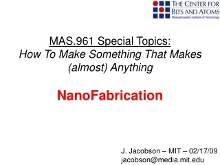
MAS.961 Special Topics:How To Make Something That Makes (almost) Anything NanoFabrication J. Jacobson – MIT – 02/17/09 jacobson@media.mit.edu
Outline • Optical Fabrication Technologies • Probe/MEMS Fabrication Technologies • Imprint Fabrication Technologies • Particle Beam Fabrication Technologies
Immersion Lithography 22-nm immersion interference lithography T. M. Bloomstein, M. F. Marchant, S. Deneault, D. E. Hardy, and M. Rothschild 10 July 2006 / Vol. 14, No. 14 / OPTICS EXPRESS 6434 Received 11 May 2006; revised 23 June 2006; accepted 23 June 2006
Immersion Lithography (Air) (Liq)
Stereolithography Speed Resolution – Two Photon
Laser CVD Mechanism: Pyrolitic (Heating in absense of O2) Chemical Vapor Deposition (500 to 2000°C local temperature). Rates: Fiber growth rates > 2 mm/s,metals and ceramics. Linear growth rate of 200 mm/s Carbon volumetric deposition rate of 50 mm3/s carbon. Materials: Cu, Au, Si, Al, W, C, WC, B, TiC, TiN, SiC, and Si3N4. http://www.me.gatech.edu/Lackey/nsfgranteesjan02.pdf
LENS (Laser Engineered Net Shaping) www.optomec.com
Outline • Optical Fabrication Technologies • Probe/MEMS Fabrication Technologies • Imprint Fabrication Technologies • Particle Beam Fabrication Technologies
Dip-Pen Nanolithography Mirkin et. al.
Contact Mode Nanoparticle AFM Hubert et.al.
Massively Parallel Dip-Pen Nanolithography with 55 000-Pen Two-Dimensional Arrays http://mass.micro.uiuc.edu/research/current/nanolithography/2006-focus-intro/slide12.html
Solder Jet 25 micron resolution http://www.microfab.com/research_areas/electronics/electronics.htm#anchor250555
Outline • Optical Fabrication Technologies • Probe/MEMS Fabrication Technologies • Imprint Fabrication Technologies • Particle Beam Fabrication Technologies
Cost Per Resolution Element The Case for Printed Electronics …Can we use this map as a guide towards future directions in fabrication?
Imprint Lithography Stephen Chou (Michigan/Princeton) et. al.
Step & Flash Lithography http://www.molecularimprints.com/Technology/technology2.html
MultiLayer Step and Flash Lithography Emerging Lithographic Technologies X, edited by Michael J. Lercel, Proc. of SPIE Vol. 6151, 61510J, (2006) · 0277-786X/06/$15 · doi: 10.1117/12.655604 Proc. of SPIE Vol. 6151 61510J-1
2 mm 200 nm Offset Liquid Embossing (OLE) Nanoparticle Inks Bulthaup et. Al. APL 79(10): 1525 (2001)
Nanomoulding with Amorphous Metals Golden Kumar, Hong X. Tang & Jan Schroers Vol 457| 12 February 2009| doi:10.1038/nature07718
Outline • Optical Fabrication Technologies • Probe/MEMS Fabrication Technologies • Imprint Fabrication Technologies • Particle Beam Fabrication Technologies
Focused Ion Beam FEI Corp.
Focused Ion Beam - Milling NanoLathe FIB Fabricated Stamps http://www.siint.com/en/technology/ion_beam_applications_e.html Toshiaki Fujii, and Takashi Kaito
Au contact pad Pt Pt nanowire SiO2 Pt Focused Ion Beam - Writing FIB Fabricated MOSFET FIB Pt CVD FIB CVD Pt (gate electrode)
E Beam Metal Melting ARCAM.Com
Electrospinning http://www.che.vt.edu/Wilkes/electrospinning/electrspinning.html https://www.uni-marburg.de/fb15/ag-wendorff/research/Electrospinning/fiber-hair http://en.wikipedia.org/wiki/Electrospinning
Objet: Ink Jet + UV Cure 16 micron layers http://www.2objet.com