Download
1 / 44
460 likes | 727 Vues
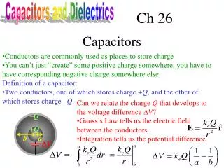
Vias and Capacitors. Chris Allen (callen@eecs.ku.edu) Course website URL people.eecs.ku.edu/~callen/713/EECS713.htm. Vias. Via, also known as plated through hole (PTH) Purpose Mounting of through-hole components (mechanical and electrical)

E N D
Vias and Capacitors Chris Allen (callen@eecs.ku.edu) Course website URL people.eecs.ku.edu/~callen/713/EECS713.htm
Vias • Via, also known as plated through hole (PTH) • Purpose • Mounting of through-hole components (mechanical and electrical) • Routing signal traces between layers (electrical) • Thermal resistance reduction (mechanical) • Different requirements for each via purpose • Issues • Mechanical tolerances and reliability • Capacitance and inductance • Via placement / return current path routing issues • Via anatomy and parameters • Pad diameter • Hole diameter • Clearance hole diameter • Plated hole diameter • Filled vias (solder, epoxy)
Via requirements • Hole diameter requirements • For mechanical vias(mounting through-hole components) • via hole diameter > lead diameter by at least 10 mils • Drilled hole diameter larger than minimum hole size • determined by plating variations • For electrical vias (not mechanical or thermal vias) • minimum via diameter is related to board thicknessT/Dvia= minimum, T = board thickness, Dvia = via diameterlimit comes from via barrel cracking (mechanical issue)Text says min T/Dvia = 5 Board manufacturers recommendmin T/Dvia 7 to 15
Via requirements • Pad diameter requirements • Pad diameter must be larger than hole diameter by a margin determined by • minimum annular ring requirement • hole diameter • hole alignment tolerance Example board manufacturers:min pad diameter 6 to 14 milsmin annular ring width 5 milsmin finished hole diameter 10 milsmin drill diameter 6 to 10 milsmin drill laser diameter 3 to 5 milsmax plated hole diameter 246 mils See example PCB fabrication capabilities and design guidelines on class website under ‘Other class documents’
Via requirements • Minimum clearance requirements • The minimum clearance between circuit elements (e.g., via pad, trace, component pad)determined several factors: • the precision of etching processrequired to yield good parts as small imperfections could lead to shorts between circuit elements • the assembly process usedwave soldering, solder bridges may be created at gaps short circuits • the minumum clearance or ‘air gap’ to avoid breakdown or arcinghigh voltages (kV) can breakdown dielectrics or air if the gap is too small • Minimum clearance may range from 2 to 20 mils depending on the process and copper thickness
Via requirements • Thermal relief vias • Power and ground planes offer low thermal resistance and act as ‘heat sinks’ • Vias for through-hole mounted components that connect to these planes often use thermal relief via pad patterns on these planes to increase the thermal resistance of the path • Examples of thermal relief via pads
Electrical effects of vias • Capacitance • Capacitance between via and ground plane or any other plane • where C is capacitance (pF)r is relative dielectric constantT is PC board thickness (inches)D1 is diameter of via pad (inches)D2 is diameter of clearance hole (inches) • this formula assumes a via pad on every layer • Typically via capacitance will be relatively small and the primarily impact will be degraded signal rise time
Electrical effects of vias • Inductance • Via inductance is approximated by • where L is inductance (nH)h is the via length (inches)d is the via barrel diameter (inches) • Note that h T from the capacitance calculation, h is the length of the via over which the signal passes
Electrical effects of vias • Example • Consider a 100-mil thick FR-4 circuit board (T = 0.1”) with a 20-mil via barrel diameter (d = 0.02”)a 30-mil via pad diameter (D1 = 0.3”)a 50-mil clearance hole diameter (D2 = 0.05”)a 20-mil via length to the power plane (h = 0.02”) • Find Cvia, Lvia, and draw the equivalent circuit
Electrical effects of vias • Effects of Lvia, Cvia • Both Lviaand Cvia result in increased signal rise time • Also Lviaincreases the impedance to the power or ground plane • Example: consider 10G GaAs technology, Tr = 150 ps, Zo = 50 Cvia = 1.02 pF, Lvia = 0.24 nH • Rise time degradation • Impedance to power plane
Vias and return current path • Recall that the return current path flows along the path of least impedance (inductance) • The proximity effect and inductance cause the return current to flow beneath the signal trace • Consider what happens when a signal changes layers through a via • The signal follows the signal trace where it can • As the signal trace changes layers, and the return current cannot, the inductance is increased • Rise time increases • Crosstalk increases
Vias and return current path • How to avoid the problem ofreturn-path current failing to shadow the signal current: • Keep all high-speed signal traces on its initial layerPractical? May be used for clock signals • Restrict signal traces to either side of a particular plane • Provide vias between ground planes at points where the signal changes layers (near signal vias) • Distribute ground vias everywhereGood for DC purposes also
Decoupling capacitors and return path • Return current plane jumping at the termination resistor, RT • To permit the return current to follow the signal, AC couple VTT plane to GND plane through decoupling capacitor, C • Placement of the decoupling capacitor depends on the power/ground plane arrangement
Decoupling capacitor placement • Using the VTT plane for return path, decoupling capacitors are placed between GND and VTT near the driver chip • Recall that in the GaAs package, the silicon chip carrier contained integrated capacitors between VTT and VDDO • Otherwise, decoupling capacitors are placed near the terminating resistor between GND and VTT
Bypass capacitors • Stable reference voltages • For CMOS and TTL logic families, the reference voltage (used to determine if an input is HI or LO) is derived from the supply voltage • Therefore a noisy supply voltage will produce a noisy reference voltage bit errors • Two questions – How can noise get into the supply voltage?How to reduce this noise? Inductive distribution system can lead to a noisy supply voltage.Transient supply currents result in voltage variations, V = L dI/dt.Similarly, an inductance can result in noise on ground reference.
Bypass capacitors • Stable reference voltages • A solution is to use ground andpower planes • To reduce the noise, follow these rules: • Use low-impedance ground between devices (R + jL) • Use low-impedance power connection between devices • Provide low-impedance path between power and ground • Clearly power and ground planes satisfy 1 & 2 • To achieve 3, need lower impedance by providing alternative path • Bypass capacitors provide low-impedance path between power and ground • Therefore locate bypass capacitors near every integrated circuit
Vias and return current path • For ECL and GaAs logic, a reference voltage (VBB) is generated on chip and this reference voltage varies only slightly with variations in Vsupply and temperature • To ensure a common reference voltage GaAs logic devices provide a VBBS output and receive as inputs VBB so that all devices share a common threshold level • Bypass capacitors are also needed with these devices ECL 2-input OR/NOR
Vias and return current path • When interfacing ECL with GaAs, the ECL device’s VBB reference level can be shared with the GaAs devices • How to determine VBB for ECL circuit? • Capacitor used to prevent oscillations • VBB is DC ~ -1.3 V • While ECL operates by current steering, i.e., it draws about the same current regardless of current state, bypass capacitors are still needed between VEE and GND to provide low-impedance path, otherwise return path goes through the Vsupply
The capacitor • Consider a physical capacitor • The equivalent circuit for this capacitor is • Therefore these can be ignored, for a simplified capacitor model • where • Ls= inductance, lead or self or equvalent series inductance, ESL (H) • Rs = equivalent series resistance, ESR () • C = capacitance (F) typically Rdiel is large (low loss)Rplate is smallClead << C
The capacitor • Consider the impedance of the capacitor model • Z = Rs + j(Ls – 1/C) • The capacitor model behaves differently depending on the frequency • At low frequencies, • Z Rs – j 1/Cbehaves like an ideal capacitor when Rs << 1/C • At resonance frequency, • Z = Rs • purely resistive over narrow frequency range • At high frequencies, • Z Rs + j Ls • behaves like an ideal inductor when Rs << Ls
The capacitor • Composite behavior • The frequency, • is called the self-resonant frequency or series-resonant frequency (SRF) • for f < fo, capacitor behaves capacitively • for f > fo, capacitor behaves inductively • In our applications (bypass and decoupling capacitors) we are seeking a low-impedance path at high frequencies • We need capacitors with self-resonant frequencies above Fknee • Otherwise, instead of a low-impedance path to a power or ground plane, we have a high-impedance path
Capacitor specifications • Real capacitors • Typical values • C: capacitor value • ESR (Rs): 1 m to 1 • ESL (Ls): 5 to 10 nH for leaded capacitors < 1 nH for leadless capacitors • Sometimes ESR is specified in terms of a dissipation factor (DF) • DF = Rs/Xc ratio of energy dissipated to energy stored per cycle • DF = ·Rs·C also includes dielectric loss (tan ) • DF = 1/Q where Q is the quality factor • Consider a 100-pF capacitor with DF of 710-5 at 100 MHz
Capacitor specifications • Most capacitors have self-resonant frequencies, fo, in the 10s of MHz to 100s of MHz • For ECL (Tr = 700 ps), Fknee = 714 MHzGaAs (Tr = 150 ps), Fknee = 3.3 GHz • To find capacitors with fo in the GHz range, must use chip capacitors • Consult RF and microwave component vendors to find these caps • Typical capacitor values are relatively small ~ 1000 pF or less • at 100 MHz, Xc = 1/(2 108 10-9) = 1.59 • at 1 GHz, Xc = 1/(2 109 10-9) = 159 m • if fo = 1 GHz, then Ls = [(2fo)2C]-1 = 25 pH
Capacitor specifications • Other capacitor characteristics • Dielectric absorption (DA) • Hystersis-like internal charge distributionresidual charge or charge density • This characteristic is a factor in sample-and-hold circuits not a factor in high-frequency decoupling • Peak working voltage (WVDC) • Limited by dielectric breakdown characteristics, orpower dissipation (heating) at the maximum frequency • Variations in capacitor value • Due to temperature – temperature coefficient, TC (ppm/C) • Due to aging or time (% change) • Due to voltage
Capacitor specifications • Dielectric materials • Capacitance value depends onarea (A), spacing between plates (d), relative dielectric constant (r) • By using various dielectric materials, different properties are obtained • The following tables list some common capacitor types using dielectric material as the distinguishing parameter
Capacitor specifications • from Horowitz and Hill, The Art of Electronics, Cambridge Press, 1989
Capacitor specifications • from Horowitz and Hill, The Art of Electronics, Cambridge Press, 1989
Capacitor specifications • from Guinta, S., “Ask The Applications Engineer – 21: Capacitance and Capacitors”, Analog` Dialogue, 30-2, pg. 21, 1996.
Capacitor specifications • from Guinta, S., “Ask The Applications Engineer – 21: Capacitance and Capacitors”, Analog` Dialogue, 30-2, pg. 21, 1996.
Capacitor selection • A variety of capacitor values are required in high-speed digital circuit designs — 100 pF to 10s of F • For low-frequency applications (DC to few MHz) — • large value capacitors, electrolytic capacitors can be used, however these have a poor frequency responseself-resonant frequency ~ few MHz • For high-frequency decoupling or bypass applications — • capacitors with high self-resonant frequencies are needed • these devices physically small chip capacitors are needed • The dielectric materials used for high-frequency applications include • Material.r. DF . • Barium titanate (BaTiO3) ~ 8000 0.1 • Alumina ~ 9 5 10-4 • Porcelain ~ 15 7 10-5
Capacitor selection • Clearly barium titanate’s (BaTiO3) large r makes it a desirable material for capacitor use • However its large dissipation factor (low Q) makes it less desirable • In addition, BaTiO3 has other disadvantages • large temperature coefficient • piezoelectric effects • poor aging characteristics • porous (moisture and chemical penetration affect performance and reliability) • lossy (tan ) • Various blends of BaTiO3 overcome some of these problems these include Z5U and X7R dielectrics that are discussed in the text • Other high-frequency capacitors use porcelain lower DF, non-porous, non-piezoelectric
Chip capacitor types • Chip capacitors come in two types • Single layer — lower capacitor values, higher self-resonant frequency • Multi-layer — higher capacitor values, lower self-resonant frequency Single-layer capacitors Multi-layer capacitor
Chip capacitor types • Parallel resonance • In addition to series resonant frequency, parallel resonance frequencies also exist due to internal inductance • One way to reduce parallel resonance is to mount capacitor on its side supporting uniform internal current distribution • However series resonance (lower freq than parallel resonance) is the limiting factor of interest
Chip capacitor types • Lower capacitance values higher resonant frequencies • ATC 100 – Case B: C = 1000 pF fo = 250 MHz C = 4 pF fo = 3 GHz • For the highest resonant frequency, use single layer capacitors • C = 1000 pF fo = 600 MHz • Which capacitor should be used? • What is the maximum frequency of interest? (Fknee) • What Xc can be tolerated? Single-layer capacitor Multi-layer capacitor
Chip capacitor types • A typical circuit board will use a variety of capacitors • A group of electrolytic capacitors (e.g., 100 µF, 10 µF, 1 µF) clustered near where the DC power enters the circuit board • Groups of bypass chip capacitors near the integrated circuits • Groups of decoupling chip capacitors whose placement depends on the board stackup • Appropriate selection of capacitor values can involve time-domain or frequency-domain analysis • Time domain: estimate the charge needed to support transient currents during switching events, and size the capacitance accordingly • Frequency domain: think of capacitors as filter and select values to provide low impedance path from power supply or power plane over DC to Fknee frequency range
Chip capacitor types • To provide the desired decoupling or bypass operationit may be necessary to use several capacitors in parallel • “An array of bypass capacitors is more effective than a single bypass capacitor.” • “Within a certain radius, all the bypass capacitors will act as if connected in parallel, lowering the power-to-ground impedance. The effective radius within which this effect works is equal to l/12 where l is the electrical length of the rising edge. All capacitors within the diameter of l/6 act in concert as a lumped circuit.”
Chip capacitor types • Assuming the decoupling capacitor passes signal components with frequencies above 10 kHz, what path do return currents follow to close the loop for signal components below 10 kHz (e.g., 1 kHz, DC)?
Chip capacitor types • Proper bypass capacitor placement
Chip capacitor types • Proper bypass capacitor placement
Chip capacitor types • Proper bypass capacitor placement
Chip capacitor types • Broadband capacitors are relatively new on the market • These offer low impedance over a broad frequency range • Achieved by integrating various capacitors within a single package 520L: C = 10 nF, 160 kHz to 16 GHz 530L: C = 100 nF, 16 kHz to 18 GHz 545L: C = 100 nF, 16 kHz to 40 GHz 550L: C = 100 nF, 16 kHz to 40 GHz
Summary • Vias serve a variety of purposes in high-speed digital circuit boards • Via parameters are driven by manufacturing and reliability issues • The capacitive effects of vias are less significant than inductive effects • Via placement can play an important role in return current path • Decoupling capacitors are used to shunt current to the return path • Bypass capacitors are used to suppress noise on power and ground • Real capacitors have resistance and inductance • Real capacitors have a self-resonant frequency (SRF) • Below the SRF it behaves capacitively • Above the SRF it behaves inductively • Groups of capacitors are used to provide a capacitive response over a broad range of frequencies