Download
1 / 49
490 likes | 655 Vues
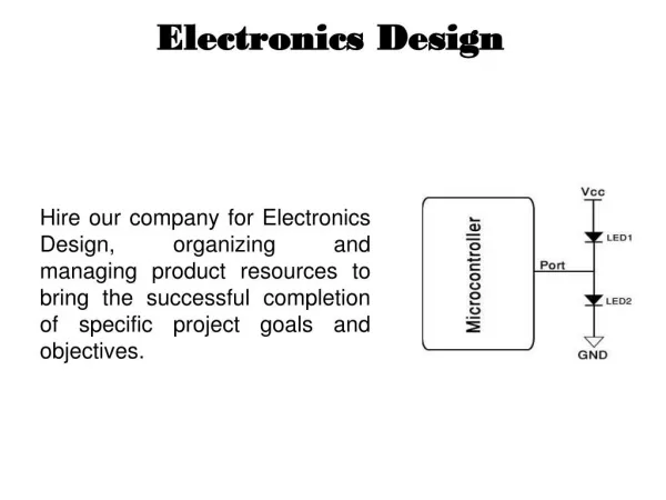
Revamping Electronic Design Process to Embrace Interconnect Dominance. Chung-Kuan Cheng CSE Department UC San Diego La Jolla, CA 92093-0404 ckcheng@ucsd.edu. Interconnect Dominance. Goals: Speed, Power, Cost Constraints: Area, Current, Skew Challenges: PVT Variations, Signal Integrity.

E N D
Revamping Electronic Design Process to Embrace Interconnect Dominance Chung-Kuan Cheng CSE Department UC San Diego La Jolla, CA 92093-0404 ckcheng@ucsd.edu
Interconnect Dominance Goals: Speed, Power, Cost Constraints: Area, Current, Skew Challenges: PVT Variations, Signal Integrity
Outlines • Interconnect Technologies • Buffers, Pitches, Circuit Styles • Geometrical Planning • Wire Orientations, Chip Shapes • Interconnect Networks • Topologies, Wire Styles • Power and Clock Distributions • Functional Modules • Adders, Shifters • Conclusion
Interconnect Technologies • RC Wires • Wire Pitch, Width, Separation • Buffer Size, Buffer Interval • Transmission Line • RLCG
Interconnect Technologies Coupling capacitance: Self capacitance: Total wire capacitance:
Interconnect Technologies SRC Roadmap 2005
Interconnect Technologies Design metrics: Objective functions: For each pitch, For each objective function Find wire width w, buffer size sinv and buffer interval linv Calculate the metrics
Experimental Results – normalized delay Top left: Overview Top right: at different pitches (solid lines: min-pitch; dash lines: saturating pitch) Bottom right: at 70nm technology
Interconnect Tech. -- bandwidth Top left: Overview Top right: at min-pitches Bottom right: at 70nm technology
Interconnect Tech. – bandwidth/power Top left: Overview Top right: at different pitches (solid lines: min-pitch; dash lines: optimal pitch) Bottom right: at 70nm technology
Interconnect Tech.: Transmission Line • Speed-of-the-light on-chip communication • < 1/5 Delay of Traditional Wires • Low Power Consumption • < 1/5 Power Consumption • Robust against process variations • Short Latency • Insensitive to Feature Size
Interconnect Tech.: Transmission Line Differential Transmission Line Surfliner • Shunt conductance compensates voltage loss: R/G = L/C. • Flat from DC Mode to Giga Hz • Telegraph Cable: O. Heaviside in 1887. • Serial resistance causes voltage loss. • Speed and attenuation are frequency dependent.
Theory (Telegrapher’s Equation) • Telegrapher’s equation: • Propagation Constant: • Wave Propagation: • Alpha and Beta corresponds to speed and phase velocity. Both arefrequency dependant
Theory (Distortionless Line) • Set G=RC/L • Frequency Independent speed and attenuation: • Characteristic impedance: (pure resistive) • Phase Velocity (Speed of light in the media) • Attenuation:
Interconnect Tech.: Transmission Line • Add shunt conductance between differential wires • Resistors realized by serpentine unsilicided poly, diffusion resistors, or high resistive metal
Geometrical Planning • Wire Orientations • Manhattan, Hexagonal, Octagonal, Euclidean • Die Shapes • Rectangle, Diamond, Hexagon, Octagon, Circle
Throughput : concurrent flow demand *ratio of 0-90 planes and 45-135 planes is not fixed
Congestion map of square chip using X-architecture 12 by 12 13 by 13
Y-architecture + Square Chip 12 by 12 13 by 13
Routing Grids Y-Architecture X-Architecture (http://www.xinitiative.org/img/062102forum.pdf)
Interconnect Networks • Optimized Interconnect Architecture • Data Bus, Control Signals • Shared Interconnect • Packet Switching • Circuit Switching • RTL Level Partition
Interconnect Networks Physical Implementation
Interconnect Networks • Obj: Power, Latency • Constraints: • Routing Area, Bandwidth • Design Space: • Topology • Wire Styles, Switches • Model: • Traffic Demand • Data Bus, Control Signals
Topology Selection (Latency, Power, BW) Optimal 8-node topologies vs area resources
Clock: Linear Variations Model • Process variation model • Transistor length • Wire width • Linear variation model • Power variation model • Supply voltage varies randomly (10%)
Clock: RC Model Input: an n level meshes and h-trees Constraint: routing area, parameter variations Objective: skew
Skew Expression • Assumptions: • T<<RsC • Rs /R <<RsC/T • Using first order • Taylor expansion ex=1+x,
Optimal Routing Resources Allocation total area level-4 level-3 level-2 level-1
Inductance Diminishes Shunt Effects • 0.5um wide 1.2 cm long copper wire • Input skew 20ps
Clock Distributions Surfliner
Functional Modules (Data Path) • Arithmetic • Algorithms • Logic • Logic Styles • Placement
Cyclic Shifter Delay: nlogn, Power: ¼ n2
Fan-out Splitting Delay: n Power: 3/16 n2
Cell Permutation • Fix the input/output stage, permute cells of intermediate stages to further improve delay. • Formulate as an ILP problem and solve by CPLEX. • Optimal solution in terms of delay • Delay/Power tradeoff Optimal Timing solution for 8-bit
Conclusion • Interconnect Technologies • Geometrical Planning • Interconnect Networks • Power and Clock Distributions • Functional Modules
Interconnect Technologies Example: w= 85nm, t= 145nm rn= 10Kohm,cn=0.25fF,cg=2.34xcn=0.585fF rw=2ohm/um, cw=0.2fF/um Optimal interval Optimal buffer size Optimal delay