Download
1 / 26
280 likes | 539 Vues
Additive Manufacturing for X-band applications. Alexej Grudiev 5/02/2014 CLIC14 workshop. Acknowledgements. BE-RF Miriam Colling Alexej Grudiev EN-MME Said Atieh Ofelia Capatina Floriane Leaux Raphael Leuxe Thomas Sahner Ignacio Santillana TE-VSC Sergio Calatroni

E N D
Additive Manufacturing for X-band applications Alexej Grudiev 5/02/2014 CLIC14 workshop
Acknowledgements • BE-RF • Miriam Colling • Alexej Grudiev • EN-MME • Said Atieh • Ofelia Capatina • Floriane Leaux • Raphael Leuxe • Thomas Sahner • Ignacio Santillana • TE-VSC • Sergio Calatroni • Ivo Wevers
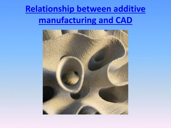
Additive manufacturing Process Model designed in CAD CAD file sent to additive manufacturing system Model divided into slices 3D product sculpted from powdered material layer by layer using the specified technique EOS – SLS, http://www.eos.info/additive_manufacturing/for_technology_interested
Technical data Ti64 Ti64 DC electrical conductivity: 600000 S/m, two times lower than stainless steel • Relatively low accuracy • Big roughness (much larger than skin depth) • Low DC conductivity Obvious RF application is a broad-band all-metal dry RF load
High power/E-field performance of Ti 30 GHz high power performance, PAC2007 DC breakdown thresholds
Three stages of the project • Low power prototype for material and fabrication characterization • DC conductivity and RF losses • UHV compatibility: leak tightness and outgassing • Shape accuracy and Roughness • Mechanical strength and Metallurgy • Prototypes for high power tests • Integration of cooling • High power performance • Design of the RF load • RF load prototype We are here
Prototype Design • Prototype modelled in HFSS • WR90 end tapered to 13mm by 2mm middle 200mm
Waveguide manufacturing methods Waveguide 1: EOS – Selective laser sintering Waveguide 2: Grenoble INP – Electron beam melting 5 Waveguides 3, 4 and 5: Concept – Selective laser melting • Length: 20cm • Material: Titanium alloy
RF measurements using VNA • Obtained data for S(1,1), S(1,2), S(2,1) and S(2,2) parameters for each of the five waveguides • Measurements required careful handling - movement in cables cause readings to change • Measurements repeated three times for each waveguide for reliable results
RF Results Comparison of S(1,1) parameter
RF Results Comparison of S(1,2) parameter
DC conductivity measurements Titanium alloy conductivity: 6E+5 S/m Two types of DC measurements: • Four probes in contact with middle section • Two probes in contact with middle while clamps on flange provide voltage difference 6mm 62mm
DC Results Titanium alloy conductivity: 6E+5 S/m Method 1 Method 2 Apply all DC cond. to HFSS waveguide and obtain values for all 3 parameters in each case aqw a Nominal HFSS values: ‘aqw’=14.2mm ‘a’=13mm Roughness=0µm
Table of parameters HFSS Nominal: a=‘13mm’ aqw=‘14.2mm’ rough=‘0um’ • Tables show: • Values for each modified parameter: ‘a’ , ‘aqw’ and HFSS roughness • 100-300 micron differences • Change in parameters required to provide HFSS results which agree with those produced by the VNA for each waveguide
Metrology Microtomography – X-ray non destructive testing 1 Radioscopic image acquisition 2 3D reconstruction 3 Post processing Images: RX solutions gallery http://www.rxsolutions.fr/#!untitled/zoom/cjjm/i47og1
Metrology Results • Blue lines show lack of material • Red lines show excess material
Metrology Results • First three waveguides were measured using microtomography to determine dimensions ‘a’ and ‘aqw’ • Measured ‘a’ at 3 points and ‘aqw’ and 2 points and an average was found • Waveguide 1 and 3 < 100micron difference from nominal RF+DC measurements:
Vacuum • Waveguide 1, 3,4 and 5 are leak tight, OK for UHV • Waveguide 2 was not be able to pump down due to presence of small holes
Mechanical testing and metallographic observations Waveguide 2 Waveguide 3 Waveguide 1 Before etching After etching W1 shows least porosity W2 shows large porosity W3 shows different microstructure
Summary of the results obtained after tensile tests of the samples OK OK
Summary • Laser melting fabrication is validated for two manufacturers • EBM fabrication requires some improvements • Next step: