
Uploaded by
nell-downs
11 SLIDES
279 VUES
120LIKES
Some PCB Layout Issues
DESCRIPTION
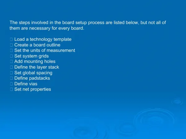
Some PCB Layout Issues. Ground Bounce. 500 mV. GND. V CCI Noise. 500 mV/DIV. V CCA Noise. 500 mV/DIV. AD Bus Signal Quality. 500 mV/DIV. V CCA /V CCI Noise Measurements. Original layout pattern for an FPGA implementing a PCI core.
Download
1 / 11
Télécharger la présentation 
Some PCB Layout Issues
An Image/Link below is provided (as is) to download presentation
Download Policy: Content on the Website is provided to you AS IS for your information and personal use and may not be sold / licensed / shared on other websites without getting consent from its author.
Content is provided to you AS IS for your information and personal use only.
Download presentation by click this link.
While downloading, if for some reason you are not able to download a presentation, the publisher may have deleted the file from their server.
During download, if you can't get a presentation, the file might be deleted by the publisher.
E N D
Presentation Transcript
Ground Bounce 500 mV GND
VCCI Noise 500 mV/DIV
VCCA Noise 500 mV/DIV
AD Bus Signal Quality 500 mV/DIV
Original layout pattern for an FPGA implementing a PCI core.
Original layout pattern for an FPGA implementing a PCI core. • Note: • Small trace width for these array power connections. • Via "islands" separating cap from FPGA


More Related