Download
1 / 1
10 likes | 110 Vues
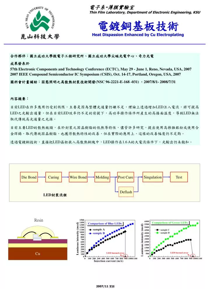
電子系 - 薄膜實驗室 Thin Film Laboratory, Department of Electronic Engineering, KSU. 電鍍銅基板技術 Heat Dispassion Enhanced by Cu Electroplating. 合作夥伴:國立成功大學微電子工程研究所、國立成功大學尖端光電中心、奇力光電 成果發表於 57th Electronic Components and Technology Conference (ECTC), May 29 - June 1, Reno, Nevada, USA, 2007

E N D
電子系-薄膜實驗室 Thin Film Laboratory, Department of Electronic Engineering, KSU 電鍍銅基板技術 Heat Dispassion Enhanced by Cu Electroplating 合作夥伴:國立成功大學微電子工程研究所、國立成功大學尖端光電中心、奇力光電 成果發表於 57th Electronic Components and Technology Conference (ECTC), May 29 - June 1, Reno, Nevada, USA, 2007 2007 IEEE Compound Semiconductor IC Symposium (CSIS), Oct. 14-17, Portland, Oregon, USA, 2007 國科會計畫補助:固態照明之高散熱封裝技術開發(NSC 96-2221-E-168 -031),2007/8/1- 2008/7/31 內容摘要: 目前LED在許多應用仍受到侷限,主要是因為整體光通量仍嫌不足,理論上透過增加LED注入電流,將可提高LED之光輸出通量,但在目前LED效率仍不足的前提下,高功率操作條件所產生的高接面溫度,導致LED無法取代傳統高光通量之光源。 目前主要LED的散熱瓶頸,在於封裝之固晶樹脂的低熱導特性,儘管許多研究,提出使用高摻雜銀粉或使用合金焊錫,取代傳統固晶樹脂,也獲得散熱特性的改善,但在實際的應用上,這樣的改善幅度仍不足夠。 透過電鍍銅技術,直接把LED晶粒嵌入高散熱銅塊中,LED操作在1.6 A的大電流條件下,光輸出仍未飽和。 Singulation Test Die Bond Curing Wire Bond Molding Post Cure Deflash LED封裝流程 2007/11 更新