On-Chip Bus Experiment and LED Flashing using FPGA and Flash Memory
This lab experiment focuses on the implementation of an on-chip bus system using FPGA and flash memory to control LED flashing. Students learn to program the FPGA using various methods, including a direct bitstream upload and a flash memory approach. The experiment involves configuring projects, generating programming files, and downloading the bitstream to observe LED behavior based on switch configurations. Additionally, students will explore how to interact with hardware via software and trace connections within an AMBA interface.

On-Chip Bus Experiment and LED Flashing using FPGA and Flash Memory
E N D
Presentation Transcript
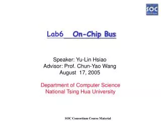
Lab6 On-Chip BUSExperiment Speaker: Yu-Lin Hsiao Advisor: Prof. Chun-Yao Wang August 17, 2005 Department of Computer Science National Tsing Hua University
Outline • Introduction ﹣Example 1 ﹣Example 2 • Exercise
Experiment Task • Flashes the LEDs on the Logic Module from left to right. • The speed of flashing the LEDs can be set by the 8-way switch. • FPGA version: program the FPGA by writing the bitstream image into the FPGA directly. The image will start running right after programming into the FPGA. • Flash version: program the FPGA by writing the bitstream into the flash. The image will start after next power up of the development system.
Step 1 • Create new project for Xilinx 4.1: (a) Device Family: VirtexE (b) Device: xcv2000e-6fg680 (c) Design Flow: XST Verilog
Step 2 • Add verilog file (Example1.v) to this project. Top module
Step 3 ★ ★ ★ • Copy user constraints file (example1.ucf) to the project directory and check the constraints. Name of user constraints file should be the same with top module!!
Step 4 • Generate the bitstream: ﹣Select Top module, ﹣Double click the Generate Programming File
Step 5 • Copy example1.bit to the directory which contains the progcards.exe file. (…/Codes/Hw/example1/download/) • Modify example1_to_flash.brd and example1_to_fpga.brd.
Step 6 • Connect ARM Multi-ICE onto LM, • Set the LM in Config Mode by shorting the CFGLNK jumper on the LM board. CFGLNK CFGLED
Step 7 • Auto-config in the Multi-ICE Server program.
Step 8 • Execute progcards.exe to download the bitstream to the FPGA.
Step 9 • Execute progcards.exe to download the bitstream to the Flash.
Step 10 • Set the LM in Normal Mode • Select the flash image to be executed. Which flash image to be executed is selected by the position of the 4-way switch S1 on the LM • Power the LM up again and observe the LM
Outline • Introduction ﹣Example 1 ﹣Example 2 • Exercise
Experiment Task • Determine DRAM size on the core module and sets up the system controller. • Check that the logic module is present in the AP expansion position. • Report module information. • Set the Logic Module clock frequencies. • Test SSRAM for word, halfword, and byte accesses. • Flash the LEDs. • Remain in a loop that displays the switch values on the LEDs.
Software (SW) • logic.c: The main C code. • logic.h: Constants. • platform.h: Constants. • rw_support.s: Assembler functions for SSRAM testing.
Phase 1 • Repeat step 1 to step 7, step 9, and step 10 above to download the bitstream (ahbahbtop.bit) to the Flash. • After finishing step 9, we have set LM in Normal Mode and selected the flash image to be executed by the 4-way switch. • Before powering up again, we first do phase 2.
Phase 2 (1/3) • Connect ARM Multi-ICE onto CM. • Power up and configure the Multi-ICE again.
Phase 2 (2/3) • Start CodeWarrior IDE. Open a new project and add the software code to this project.
Phase 2 (3/3) • Hit run bottom, it will start the AXD debugger.
Outline • Introduction ﹣Example 1 ﹣Example 2 • Exercise
Exercise • To trace the hardware code and software code, indicate that software how to communicate with hardware using the AMBA interface. • If we want to design an accumulator ( 1,2,3,… ), how could you do to implement it using the scratch code? • In example 1, explain the differences between the Flash version and the FPGA one.