Download
1 / 20
210 likes | 394 Vues
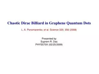
Chaotic Dirac Billiard in Graphene Quantum Dots L. A. Ponomarenko, et al. Science 320, 356 (2008) Presented by Suprem R. Das PHYS570X (02/25/2009). Important findings of the paper: 0D graphene Nanoelectronics/transport study All graphene SET/QD first report

E N D
Chaotic Dirac Billiard in Graphene Quantum Dots L. A. Ponomarenko, et al. Science 320, 356 (2008) Presented by Suprem R. Das PHYS570X (02/25/2009)
Important findings of the paper: 0D graphene Nanoelectronics/transport study All graphene SET/QD first report Both SET and QD regime studied Graphene QD Dirac fermion statistics study (Q cap 1/D for D > 100 nm but 1/D2 for smaller dots, quantum chaos and neutrino billiards) Very small Dot (~ 1nm) Room temperature Graphene QD transistor action – possibility of graphene based molecular electronics (top down approach)
Quantum Dots: Artificial structures consisting of Size ~ 100 nm or less (> 100 nm: SET) Semiconducting materials, small molecular clusters, small metallic grains – all having similar transport properties # of free e in the dot – very small (~ 1 to few hundred) Few characteristics of QDs (otherwise called artificial atoms) • For these electrons de Brog ~ dot size and electrons occupy discrete quantum levels (similar to atomic orbitals in atoms) and have a discrete excitation spectrum • Charging energy (analogous to ionization energy of atom) – energy required to add/remove a single electron from the dot • The atom-like physics of dots is usually studied by measuring their transport properties (attaching current and voltage leads to probe the dot’s states)
Coupling of S/D contacts with the iland through particle exchange and coupling of G with the iland through electrostatic or capacitive coupling
Conditions/assumption to achieve a QD Formation of a well defined iland, such that total charge inside the iland is an integer (Ne, say), when no coupling to S/D. Tunneling to S/D => N adjusts itself until the energy of the whole circuit gets minimized, charge on the iland suddenly changes by the quantized amount e Change in the Electrostatic potential energy/ Coulomb energy of the iland is called charging energy EC = e2/C, where C is the capacitance of the iland. EC (charging energy) becomes important when EC > kBT The barriers are sufficiently opaque such that the electrons are located either in S,D, or the CI => Quantum fluctuations in N due to tunneling through the barriers << 1/(time scale of measurements), where time scale of measurement = e/current. Above requirement sets a lower limit for the tunnel resistances Rt of the barriers
If Rt the lower limit for tunnel resistance, C the capacitance for the dot, then t = charging/discharging time for the dot = RtC • Applying Heisenberg’s Uncertainty principle to the dot: E t > h => (e2/C).(RtC) > h => Rt >> h/e2, the resistance quantum (25.813k) If Rt ~ h/e2, then energy uncertainty will not be smaller than charging energy to see the effect.
Two conditions for observing effects due to discrete nature of charge: • Rt >> h/e2 Achieved by weakly coupling the dot to S/D (using side gates) • EC >> kBT or e2/C >> kBT Achieved by making the dot smaller, since C R, the radius of dot (the dot can be squeezed by applying potential to the central pair of gates) Note of T regimes: • e2/C << kBT (high T limit), discreteness of charge cannot be seen, G is independent of dot size, and electron numbers, and is ohmic sum of 2 barrier conductances • E << kBT << e2/C, the classical or metallic Coulomb blockade regime, where many levels are excited by thermal fluctuations • kBT << E < e2/C, the quantum Coulomb blockade regime, where only one or a few levels participate in transport Ref: L. P. Kouwenhoven, C.M. Marcus et al., Proc of Adv Study Institute on Mesoscopic Electron Transport (Kluwer 1997)
Coulomb Oscillations (I – VG measurements at fixed VDS) and Coulomb Staircase (I – VDS measurements at fixed VG) Tunneling changes the iland’s charge by an integer while the gate voltage VG induces an effective continuous charge q=CGVG If we sweep VG, the build up of the induced charge will be compensated in periodic intervals by tunneling of discrete charges onto the dot This competition between the continuously induced charge and discrete compensation leads to Coulomb Oscillations (usually, plotted between conductance G (= I/VDS) in units of e2/h vs VG) Plot of I vs VDS for particular VG is called Coulomb staircase. A new current step occurs at a threshold voltage (~e2/C) at which an extra electron is energetically allowed to enter into the iland
Ref: L.P. Kouwenhoven et al, Physica B249-251 (1998) 191 M. Kastner, MIT, Physics Today article
Graphene QD Device Geometry Patterned on Si/SiO2 (300 nm) using EBL
Findings: Three basic operational regimes for QDs, depending on the diameter D. D > 100 nm: Conventional SET, characterized by periodic Quolomb Blockade peaks 100 nm < D < few nm: A QD having quantum confinements characterized by strong non-periodic peaks, random peak spacings ---statistics fitted to chaotic neutrino billirds Short constrictions ~ few nm: Conductive with confinement gap of up to 0.5eV – possibility of top down approach of graphene molecular electronics
Low T: Coulomb resonance peaks separated by regions of zero conductance (D = 250 nm, T = 0.3K, Measurements around VG~ 15V) High T: peaks become broader and overlap, gradually transforming into CB oscillations (D = 250 nm, T = 4K, Measurements over large VG)
OBSERVATIONS • Periodicity in CB resonance peaks • Variations in CB peak heights attributed to interference-induced changes in barrier transparency • Oscillations become weaker as G increases with carrier conc or T • Oscillations completely disappear for G > ~0.5 e2/h => Transparent enough barriers to observe CB • More than ~ 1000 oscillations with VG ~ 16mV => CG = e/ VG ~ 10aF, which is order of expected value (CG ~ 20 (+1) D ~ 20 aF with ~ 4 and D ~ 250nm), the difference being accounted for the screening by the contact regions • Overall G vs VG resembles that of large graphene sheet
Results for devices with D < 100nm (QD) • OBSERVATIONS • <VG> - average peak separation, (VG) – standard deviation in average peak separation • CB peak are non periodic and varied strongly in spacing with smaller dots • Height of the coulomb diamond varied with D • Variation in VG is more than order of magnitude for typical nongraphene QDs => Size quantization is important for graphene based QDs • E (CB peak spacing) = EC (charging energy) + E (confinement energy or level spacing), and EC is constant for a given dot geometry • For massive electrons E~ h2/8mD2, for massless Dirac fermions E~ vFh/2D • In this case, for D~40nm, E~ /D ~ 10meV ( ~ 0.5 eV.nm, by a factor 2 according to different model) D = 40 nm C: Variation of VG over 140 n.n. peaks obtained over a wide range of VG for 40 nm dot biased at zero Vb
However... E = EC + E and we know Ec 1/C(geomet) and E C(Quantum) And Geometrical Cap D and Quantum capacitance 1/D => E or < VG> 1/D But analysis of Q.Cap. Vs D shows the following Blue (solid line): <VG> 1/D : fits well above 100nm but not below Red (dashed line): <VG> 1/D2 Green (dotted): <VG> 1/D with = 1.25: Fits well in all D
Another Observation: Notable change in shape of the spectral distribution below D ~ 100nm Statistical analysis of peak spacing for four QDs with different D
Results for QD devices with D < 30 nm • OBSERVATIONS • Completely dominated by Quantum confinement • Insulating regions in VG as large as several V • Level spacing exceeding ~ 50 meV (from stability diagram) • Experimental conditions are uncontrollable for very small feature size => effects of multi dots or individual QPC, or sometimes residual photoresist affects the results • Still using E ~ /D with ~ 0.5 eV.nm and E ~ 40meV => D ~ 15nm
Results for very small QD devices (D ~ 1 nm) • OBSERVATIONS • Further increase in Eachieved by reducing size using plasma etching (smallest device) • Room T transistor action (GOFF < 10-10 S, GON ~ 10-3 e2/h) • At large biases, conductance onset shifting with Vb • Estimated E ~ 0.5 eV => D ~ 1nm • At low T, no switching • Fluctuations in the signal • Presence of occasional transmission resonances • Origin of switching not known
Comments & Conclusions • In extremely small scales, any kinds of irregularities in the structure are neither controllable nor can be studied properly • CB and confinements are all based on particle nature of the carriers, but the interference effects arising from the wave nature of electrons not studied • At very small scale, Dirac fermions’ interactions may be prominent but their effect here is not discussed