Configuration of FPGA Using Flash Memory: Project Overview and Implementation Details
This project focuses on leveraging FLASH memory for configuring FPGA systems, primarily utilizing VHDL on an Altera Cyclone II FPGA. It outlines the project's goals such as enhancing system component configuration, implementing a robust data structure for storage and transmission, and enabling host interaction with FLASH data. The architecture incorporates UART communication and Wishbone protocol for internal data transfer. With built-in debugging capabilities, this work aims to establish a reliable framework for FPGA settings, providing insights on GUI development and testability.

Configuration of FPGA Using Flash Memory: Project Overview and Implementation Details
E N D
Presentation Transcript
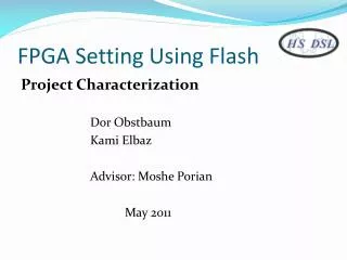
Dor FPGA Setting Using Flash 0.5 Project Characterization Dor Obstbaum Kami Elbaz Advisor: Moshe Porian May 2011
Dor Contents 0.5 • Project Overview • Project Goals • Requirements • Architecture • Micro Architecture • Testability & GUI • Schedule
Dor Project Overview 2 • Why do we need FPGA setting using FLASH? • One VHDL file operating with different configurations • Software independency FLASH FPGA Client Client GUI Client
Dor Project Goals 0.5 • Configure system components using data stored in FLASH. • Implementing a data structure that will be used for data storage in FLASH and for data transmission to clients. • Setting an option for a host to read data from FLASH and write new data to it. • Implementing strong debugging capabilities.
Dor Requirements 0.5 • VHDL Implementation • DE2 development board that features an Altera Cyclone II FPGA • FPGA – Host communication via UART protocol • Internal communication via Wishbone protocol
Dor Architecture 3
Dor Regular data transfer 1.5
Dor Wishbone & wishbone intercon 2.5
Dor Filter
Dor Clk&Reset
Dor Flash control 1
Kami Leds - Client
Sys_clk 100 MHz Timer Time unit Time unit frequency Num_of_tics = Counter
Kami Leds - Client
Kami Display - Client
For example… Row_En Column_En Resolution 1024 x 768 Damka_En Row_En 8 Row_Val = 128
UARTProtocol start parity stop 8 bit word
Kami RX Path
Kami TX Path
Kami GUI & Testability
Kami Schedule
Kami Schedule