Download
1 / 23
320 likes | 766 Vues
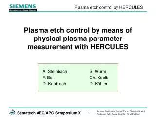
Plasma etch control by means of physical plasma parameter measurement with HERCULES. A. Steinbach S. Wurm F. Bell Ch. Koelbl D. Knobloch D. Köhler. Contents. Introduction - Motivation Plasma monitoring tool HERCULES Al etch on LAM TCP 9600 SE

E N D
Plasma etch control by means of physical plasma parameter measurement with HERCULES A. Steinbach S. Wurm F. Bell Ch. Koelbl D. Knobloch D. Köhler
Contents • Introduction - Motivation • Plasma monitoring tool HERCULES • Al etch on LAM TCP 9600 SE • Contact etch on Applied Materials Centura MxP+ • Summary
Our way of plasma processing today – an effective way ? Process parameters powerpressureB fieldgas flow...... Process results etch rateuniformityselectivityparticles....... „Black Box“ called plasma processing • Experience and statistical methods in process development • “Process Monitoring” and Tool control by test wafers
rf probe rf voltagerf currentpower Process parameter rf voltage (wafer)rf currentbias voltageeffective power Species in the volume ion densityion temperatureneutral densitiesneutral temp.excitations We begin to measure ! ProcessResultsexternalmeasured etch rateuniformityselectivityparticles Processparametersexternal powerpressureB fieldgas flowbody temp. Plasma excitationPower balance and potential distribution electron collision rate, electron energy distributionelectron densityplasma potentialbulk power Wafer Surface ion energyion currentradiationneutral flows (radicals)surface temp.layer thickness Chamber parameters surface temp.polymer e.g. gas ad / desorption depending on ion current InterferometryReflectence spectroscopylayer thickness Ion flux probe j+ (wall) Hercules ne, e, PBulk OESk*i( ) Measuring Techniques for real time Plasma Monitoring
Basic HERCULES Model High Frequency Electron Resonance Current Low PressureSpectroscopy
Principle and experimental setup Algorithm • Passive electrical method,no influence on the plasma • Integral measurement
SEERS provides reciprocally averaged parameters Self Excited Electron Resonance Spectroscopy
TCP: Al etch - trend analysis main etch • Cl2 - MFC failure - Cleans
TCP: Al etch in Cl2 - first wafer effect First wafer effect in main etch
TCP: Al etch - with / without barrier (TiN,Ti) Ti layer detected
MxP+: CT etch: Plasma parameters dependíng on process parameters Change of process chemistry strong nonlinear correlation
MxP+: CT etch - Etch rate BPSG (blanket) depending on plasma parameters Obvious correlations between etch rate and electron collision rateelectron densitybulk power
MxP+: CT etch - Contact angle depending on plasma parameters Change of process chemistry no obvious correlation between electron density and contact angle
MxP+: Chamber monitoring of contact etch processes on product wafers Process mix in Applied Materials Centura MxP+ chamber: Oxide and Nitride etch with CF4 / CHF3 / Ar / O2 chemistry Process 1 Process 2 Process 3 Descum --- N2 / O2 --- Step 1 BPSG BPSG Oxide Step 2 --- Nitride ---
MxP+: CT etch - Chamber monitoring of product wafers: electron collision rate Electron collision rate • decreases with rf hours • very sensitive to etch chemistry Pr1Pr2 ! One point - one wafer
MxP+: CT etch - Chamber monitoring on product wafers: electron density Electron density • decreases with rf hours slightly • sensitive to etch chemistry One point - one wafer
MxP+: CT etch - Chamber monitoring on product wafers: bulk power Bulk power • decreases with rf hours • very sensitive to power input • nearly not sensitive to etch chemistry One point - one wafer
MxP+: CT etch - Chamber monitoring on blanket BPSG wafers • Electron collision rate correlates with uniformity. • Electron density and bulk power too
MxP+: Conditioning after wet clean Wetclean Stable chamber conditions after about 10 wafers.
MxP+: CT etch - short term chamber drift depending on idle time Electrical failure counts at Contact etch Bad chamber Wafer • Collision rate shows dependence on chamber idle time. • Constant chamber conditions after about 40 min. • Change in electron collision rate corresponds to change in electrical failure counts.
eMxP+: Arcing detection Arcing between e - chuck and wafer
Summary • Al etch in LAM TCP 9600 SE, oxide and nitride etch in Applied Materials Centura MxP+ have been monitored with HERCULES. • The measured parameters depend significantly on chamber conditions and etch results. • The masured parameters are absolute values. • No difficult modeling by the user is necessary, results are immediate.
Applications of the tool • Development and optimizing processes yes • Long and short term tool stability yes • Tool matching yes • Control of chamber cleaning yes • Control of power coupling into plasma yes • Endpoint detection possible • Layer resolution possible • Spatial resolution no • Reduction of test- and monitor wafers yes • Detection of tool failure yes • Arcing detection yes