Download
1 / 17
170 likes | 201 Vues
Explore the merger of nanophase with microstructures in materials science, leveraging LSU's capabilities. Discover nano and micro integration, from nanotube RAM to crossed Si nanowire transistors. Dive into bio-mediated crystal growth, nanowire lasers, hierarchically-ordered oxides, and more. Witness the advancements in nanotechnology for bio and device-related applications.

E N D
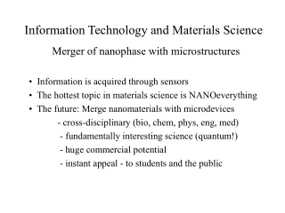
Information Technology and Materials Science Merger of nanophase with microstructures • Information is acquired through sensors • The hottest topic in materials science is NANOeverything • The future: Merge nanomaterials with microdevices - cross-disciplinary (bio, chem, phys, eng, med) - fundamentally interesting science (quantum!) - huge commercial potential - instant appeal - to students and the public
What is “Merger of Nano and Micro?” “I don’t know - but I know it when I see it.” A recent National Academy of Sciences Sackler Colloquim focused on the topic The next few slides give examples of NANO science “Shaping the world atom by atom” Quantum corral of 48 Fe atoms on Cu. The Cu surface state scatters and produces an oscillation in charge density (IBM)
Molecular Electronics - Non-volatile Nanotube RAM • Flexible nanotube ropes • Contact made when addressed by 2 electrodes • Switchable between 2 states • High density 1012/cm2 C.M. Lieber, Science
Directed Assembly - Networks of Nanostructures • Fluid flow to align 1-D nanostructures • Chemical patterning to give preferred bonding: NH2-termination attracts Si, InP, and GaP nanowires - CH3 repels • Crossed structures can be made: junctions C.M. Lieber, Science
Nanotube Nanotweezers • Electrically operated • Nano-scale manipulation • Used to pick up micron particles Size bar 1 micron C.M. Lieber, Science
Crossed Si nanowire transistor • 20-50 nm dia Si nanowires • Self assembly into transistor • Much smaller junction than current chip technology C.M. Lieber, Science
Nanotubes as Transistors • Multiwalled nanotube “ropes” have varying electrical properties • Electrical breakdown can be used to select the tube with correct properties • Transistor “tuning” Ph. Avouris, Science
Detection of Biological and Chemical Species Chemical functionalization of Si nanowire pH Sensor Protein detection: biotin functionalization allows detection of streptavidin C.M. Lieber, Science
Biologically mediated crystal growth • Unknown protein selectively determines crystal phase formed • Isolate protein+desired crystal phase • PCR • Refine • Result gives highly selective bio-mediated crystal growth • Large number of crystals can now be grown A. Belcher, Nature
Lab on a Chip • Microfabrication • Microfluidics • Biomedical applications S. Soper, M Murphy, LSU
Biomolecular Motor • F1-ATPase motor • Rotates in response to the synthesis/hydrolysis of ATP • F > 100 pN - big for such a little guy! C.D. Montemagno, Cornell Integration into a cell
Polarized Luminescence • InP nanowires exhibit highly polarized luminescence • Applications in optical communication • Photonic circuitry C.M. Lieber, Science
Nanowire Nanolasers • ZnO nanowire arrays grown on sapphire • Each individual wire is a laser • Room temperature operation • Optical computing, information storage, microanalysis P. Yang, Science
Hierarchically-ordered Oxides • Micromolding and latex-sphere templating • Structural ordering at multiple discrete length scales (in this case, 10, 100, and 1000 nm) • various compositions, silica, niobia, and titania, G. Whitesides, Science
Magnetic nanospheres and rods: Co • Solution phase synthesis • Highly controlled tight size distribution • Size-tunable magnetic properties (quantum effects) • Spheres in spintronic devices - hard disk sensors • Rods for vertical magnetic data recording Scale bar 100 nm A.P. Alivisatos, Science
Colloidal Crystals: Templates for New Materials • Almost a “lost wax” technique • Make “crystals” of solid, hollow or coated spheres • Many materials possible V.L. Colvin, Science
Current efforts: Synthesis of nano Characterization Assembly of nano Integration into devices Sensors to provide info Actuators / Motors Analytical applications Leverage LSU’s Materials Science Capabilities see www.materials.lsu.edu Recommendation: Nanotechnology especially in bio / device-related Nanomaterials for Information TechnologyNew Materials and Devices to Sense the World