Download
1 / 17
170 likes | 310 Vues
This presentation by Zhangxi Tan, Krste Asanovic, and David Patterson delves into RAMP Gold, an emulation model designed for Parlab manycore architectures. It focuses on the distinction between functional and timing models, highlighting key improvements for efficient FPGA utilization. Insights on implementing a single-socket tiled manycore, leveraging SPARC v8, and achieving a high-density design are discussed. The team addresses challenges in performance, scalability, and effective storage of CPU states within the constraints of FPGA systems.

E N D
RAMP Gold Update Zhangxi Tan, KrsteAsanovic, David Patterson UC Berkeley August, 2008
Timing Model Pipeline Functional Model Pipeline Arch State Timing State A functional model for RAMP Gold ParlabManycore • RAMP Gold: A RAMP emulation model for Parlabmanycore • Single-socket tiled manycore target • SPARC v8 -> v9 • Split functional/timing model, both in hardware • Functional model: Executes ISA • Timing model: Capture pipeline timing detail (can be cycle accurate) • Host multithreading of both functional and timing models • Built on BEE3 system • Four Xilinx Virtex 5 LX110T Functional model implementation in this talk
A RAMP Emulator • “RAMP blue” as a proof of concept • 1,008 32-bit RISC core on 105 FPGAs of 21 BEE2 boards • A bigger “RAMP blue” with more FPGAs for Parlab? • Less interesting ISA • High-end FPGAs cost thousands of dollars • CPU cores (@90 MHz) are even slower than memory! • Waste memory bandwidth • High CPI, low pipeline utilization • Poor emulation performance/FPGA • Need a high density and more efficient design
RAMP Gold Implementation • Goal : • Performance : maximize aggregate emulated instruction throughput(GIPS/FPGA) • Scalability: scale with reasonable resource consumption • Design for FPGA fabric • SRAM nature of FPGA: RAMs are cheap! • Efficient for state storage, but expensive for logic (e.g. multiplexer) • Need reconsider some traditional RISC optimizations • By passing network is against “smaller, faster” on FPGAs • ~28% LUT reduction, ~18% frequency improvement on SPARC v8 implementation, wo result forwarding • DSPs are perfect for ALU implementation • Circuit performance limited by routing • Longer pipeline • Carefully mapped FPGA primitives • Emulation latencies: e.g. across FPGAs, memory network • “High” frequency (targeting 150 MHz)
X Y IR PC 1 PC 1 PC 1 PC 1 Host multithreading CPU1 CPU2 CPU63 CPU64 Target Model Functional model on FPGA ALU GPR1 GPR1 I$ DE GPR1 GPR1 D$ +1 Thread Select 6 6 6 • Single hardware pipeline with multiple copies of CPU state • Fine-grained multithreading • Not multithreading target
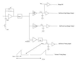
Pipeline Architecture • Single issue in order pipeline (integer only) • 11pipeline stages (no forwarding) -> 7 logical stages • Static thread scheduling, zero overhead context switch • Avoid complex operations with “microcode” • E.g. traps, ST • Physical implementation • All BRAM/LUTRAM/DSP blocks in double clocked or DDR mode • Extra pipeline stages for routing • ECC/Parity protected BRAMs • Deep submicron effect on FPGAs
Implementation Challenges • CPU state storage • Where? • How large? Does it fit on FPGA? • Minimize FPGA resource consumption • E.g. Mapping ALU to DSPs • Host cache & TLB • Need cache? • Architecture and capacity • Bandwidth requirement and R/W access ports • host multithreading amplifies the requirement
State storage • Complete 32-bit SPARC v8 ISA w. traps/exceptions • All CPU states (integer only) are stored in SRAMs on FPGA • Per context register file -- BRAM • 3register windows stored in BRAM chunks of 64 • 8 (global) + 3*16 (reg window) = 54 • 6 special registers • pc/npc -- LUTRAM • PSR (Processor state register) -- LUTRAM • WIM (Register Window Mask) -- LUTRAM • Y (High 32-bit result for MUL/DIV) -- LUTRAM • TBR (Trap based registers) -- BRAM (packed with regfile) • Buffers for host multithreading (LUTRAM) • Maximum 64 threads per pipeline on Xilinx Virtex5 • Bounded by LUTRAM depth (6-input LUTs)
Mapping SPARC ALU to DSP • Xilinx DSP48E advantage • 48-bit add/sub/logic/mux+ pattern detector • Easy to generate ALU flags: < 10 LUTs for C, O • Pipelined access over 500 MHz
DSP advantage • Instruction coverage (two DSPs / pipeline) • 1 cycle ALU (1 DSP) • LD/ST (address calculation) • Bit-wise logic (and, or, …) • SETHI (value by pass) • JMPL, RETT, CALL (address calculation) • SAVE/RESTORE (add/sub) • WRPSR, RDPSR, RDWIM (XOR op) • Long latency ALU instructions (1 DSP) • Shift/MUL (2 cycles) • 5%~10% logic save for 32-bit data path
Host Cache/TLB • Accelerating emulation performance! • Need separate model for target cache • Per thread cache • Split I/D direct-map write-allocate write-back cache • Block size: 32 bytes (BEE3 DDR2 controller heart beat) • 64-thread configuration: 256B I$, 256B D$ • Size doubled in 32-thread configuration • Non-blocking cache, 64 outstanding requests (max) • Physical tags, indexed by virtual or physical address • $ size < page size • 67% BRAM usage • Per thread TLB • Split I/D direct-map TLB: 8 entries ITLB, 8 entries DTLB • Dummy currently (VA = PA)
Cache-Memory Architecture • Cache controller • Non-blocking pipelinedaccess (3-stages) matches CPU pipeline • Decoupled access/refill: allow pipelined, OOO mem accesses • Tell the pipeline to “replay” inst. on miss • 128-bit refill/write back data path • fill one block in 2 cycles
Example: A distributed memory non-cache coherent system • Eight multithreaded SPARC v8 pipelines in two clusters • Each thread emulates one independent node in target system • 512 nodes/FPGA • Predicted emulation performance: • ~1 GIPS/FPGA (10% I$ miss, 30% D$ miss, 30% LD/ST) • x2 compared to naïve manycore implementation • Memory subsystem • Total memory capacity 16 GB, 32MB/node (512 nodes) • One DDR2 memory controller per cluster • Per FPGA bandwidth: 7.2 GB/s • Memory space is partitioned to emulate distributed memory system • 144-bit wide credit-based memory network • Inter-node communication (under development) • Two-level tree network to provide all-to-all communication
Project Status • Done with RTL implementation • ~7,200 lines synthesizableSystemverilog code • FPGA resource utilization per pipeline on Xilinx V5 LX110T • ~3% logic (LUT), ~10% BRAM • Max 10 pipelines, but back off to 8 or less for timing model • Built RTL verification infrastructure • SPARC v8 certification test suite (donated by SPARC international) + Systemverilog • Can be used to run more programs but very slow • (~0.3 KIPS)
Verification in progress • Tested instructions • All SPARC v7 ALU instructions: add/sub, logic, shift • All integer branch instructions • All special instructions: register window, system registers • Working on: LD/ST and Trap • More verification after P&R and on HW • work with the rest RAMP Gold infrastructure • Lessons so far • Infrastructure is not trivial, and very few sample design available (have to build our own!) • Multithreaded states complicates the verification process! • buffers and shared FU interfaces