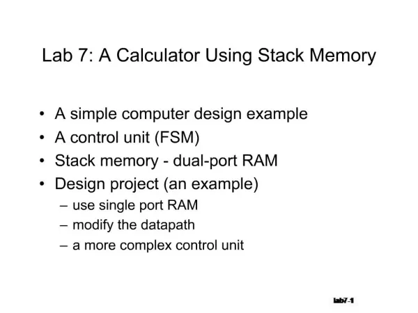
Lab 7: A Calculator Using Stack Memory
Motivation. . Computer Design as an application of digital logic design procedure. Computer = Processing Unit Memory System. Processing Unit = Control Datapath. Control = Finite State Machine. Inputs = Machine Instruction, Datapath Conditions. Outputs = Register Transfer Co

Lab 7: A Calculator Using Stack Memory
E N D
Presentation Transcript
1. Lab 7: A Calculator Using Stack Memory A simple computer design example
A control unit (FSM)
Stack memory - dual-port RAM
Design project (an example)
use single port RAM
modify the datapath
a more complex control unit
7. A stack computer
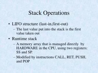
stack: a last-in-first-out queue
operand registers: the top of the stack
simple instruction encoding
easy implementation
Instruction/data format
9 bits
bit 8 = 1
bit 7-0: operation code
bit 8 = 0
bit 7-0: data (127~-127, two�s complement)
postfix format
3, 5, 8, 6, - (3�H100), +, + (3�H101), EOF (3�H1FF)
8. Block Diagram and Basic Function Basic components
dual-port RAM (stack)
one port for instruction access; the other for stack operation
IR, BREG, AREG, ALU
9. An example An example: 3, 5, 8, 6, -, +, +
10.
11. The block diagram
12. Dual-port RAM
16 * 9 bits
inputs
DI: data input
WE: write_enable (active high)
WCLK: synchronous RAM - positive-edge triggered
A: primary port r/w address
DPA: dual port read address
outputs
AO: primary port output
DPO: dual port output
primary port: stack access for data
stack pointer: an up-down counter
dual port: program access
program counter: an up counter
13. Stack pointer
push/write operation
address = stack pointer ++
pop/read operation
address = -- stack_pointer
4-bit up down counter
input: ACLR, CLK, CLK_EN, UP_DWN_
output:
CNTI: stack pointer
CNTO:
stack pointer for push
stack pointer - 1 for pop
possible problems
longer propagation delay
-1 + RAM access
14. Data Flow
15. Operations Pipelining
Fetch Exec
Fetch Exec
Fetch Exec
Execution
operation code
execute the operation
if available, pop data from the stack to A register (a memory read)
data
if A register contains data, push to the stack (a memory write)
if B register contains data, shift to A register
shift the data in IR to B register
a dual-port memory is required
one for fetching
one for execution
16. FSM for the Control Unit States
S0
S1
one operand
S2
two operands
S3
>= two operands
S4
>= three operands
Error
Halt
Operations
fetch
shift
push/pop
execution
17. Controls Inputs
RESET: power-on reset
IR: instruction register
STP: stack pointer
Outputs
AB_SEL: select the inputs for registers A and B
0/1= push/pop
A_CLK_EN, B_CLK_EN
Latch regs A andB
EOF_ = ~(IR == 1FF)
ERROR_: syntax error
IR_CLK_EN: latch IR
STP_up_dn_: 0/1 = pop/push
STP_CLK_EN: real push/pop
18. Operations and Controls fetch: IR_CLK_EN
shift: B_CLK_EN, (A_CLK_EN), !AB_SEL
push: STK_UP_DN_, STK_CLK_EN
pop: !STK_UP_DN_, STK_CLK_EN,A_CLK_EN
execution: AB_SEL, B_CLK_EN
halt: !HALT_
19. Final Design
20. Lab Download an example project
The control-unit is incomplete
You can do timing verification
Perform timing verification
Answer a couple of questions
Design the control-unit
An FSM
Implement the calculator on the demo board
Display the result using the 7-seg LEDs
21. Dual Port RAM assign AO = q[A] ;
assign DPO = q[DPA] ;
always @(posedge WCLK or posedge RST)
if (RST)
begin
q[0] = 9'h002 ;
q[1] = 9'h003 ;
q[2] = 9'h007 ;
q[3] = 9'h002 ;
q[4] = 9'h009 ;
q[5] = 9'h100 ;
q[6] = 9'h100 ;
q[7] = 9'h101 ;
q[8] = 9'h002 ;
q[9] = 9'h008 ;
q[10] = 9'h100 ;
q[11] = 9'h100 ;
q[12] = 9'h101 ;
q[13] = 9'h1ff ;
end
else if (WE)
q[A] = DI ;