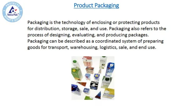
Packaging
Packaging. ECE/ChE 4752: Microelectronics Processing Laboratory. Gary S. May April 8, 2004. Outline. Introduction Test Structures Final Test Package Types Attachment. IC Manufacturing. Manufacturing = process by which raw materials are converted into finished products IC manufacturing:

Packaging
E N D
Presentation Transcript
Packaging ECE/ChE 4752: Microelectronics Processing Laboratory Gary S. May April 8, 2004
Outline • Introduction • Test Structures • Final Test • Package Types • Attachment
IC Manufacturing • Manufacturing = process by which raw materials are converted into finished products • IC manufacturing: • Inputs = wafers, insulators, dopants, metals • Outputs = ICs, systems • Processes = oxidation, deposition, photolithography, etching, doping, etc.
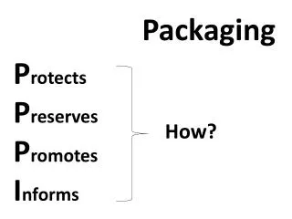
Other Key Processes • Electrical testing: necessary to ensure conformance to specifications and the reduction of any variability in the manufacturing process • Packaging: set of technologies that connect ICs with electronic systems (Analogy: “brain” = IC; “body” = package).
Outline • Introduction • Test Structures • Final Test • Package Types • Attachment
Process Control Monitors • Special structures used to assess the impact of defects • Include single transistors, single lines of conducting material, MOS capacitors, and interconnect monitors • Product wafers contain several PCMs distributed across the surface
Interconnect Test Structures • Used to assess presence of defects, which can be inferred by shorts or opens found using resistance measurements. • Meander: facilitates the detection of opens • Double comb: used to detect shorts • Various combinations of widths of lines and spaces in these test structures allow the collection of statistics on defects of various sizes.
Outline • Introduction • Test Structures • Final Test • Package Types • Attachment
Functional Testing • Final arbiter of process quality and yield • Automated test equipment (ATE) used to apply a measurement stimulus and record the results • Major functions of ATE: • Input pattern generation • Pattern application • Output response detection
Schmoo Plot • Outlined shaded region = where the device is intended to operate • Blank area outside = failure region
Cell Maps • Show failure patterns and defect types.
Die Separation • After functional testing, ICs (or dice) must be separated from the substrate. • Substrate wafer is mounted on a holder and scribed in both the x and y directions using a diamond scribe. • Wafer is removed form the holder and placed upside-down on a soft support. • Roller used to apply pressure, fracturing wafer along scribe lines • This must be accomplished with minimal damage to the individual die • Modern processes use a diamond saw, rather than a diamond scribe • Separated dice are ready to be placed into packages
Outline • Introduction • Test Structures • Final Test • Package Types • Attachment
Packaging Hierarchy • Level 0: on-chip interconnections • Level 1: inter-chip interconnections • Level 2: chip-to-PCB or chip-to-module • Level 3: board-to-board interconnections • Levels 4, 5: connections between sub-assemblies and systems (i.e., computer to printer)
Dual In-line Package (DIP) • Package most people think of when they envision ICs. • Developed in the 1960S, has long dominated the packaging market. • Can be made of plastic or ceramics
Surface Mount Package • Developed in 1970s and 1980s • Leads don’t penetrate the PCB; so package can be mounted on both sides of the board, allowing higher density. • EXAMPLE: Quad flatpack (leads on all 4 sides to increase possible I/O connections)
Pin/Ball Grid Arrays • PGAs have I/O density of ~ 600 • BGAs have densities > 1000 (compared to ~ 200 for QFPs). • BGA takes up less space than QFP, but is more expensive to manufacture.
Chip Scale Packages • Defined as packages no larger than 20% greater than the size of the IC • Designed to be flip-chip mounted • Manufactured in a process that creates power and signal I/O contacts and encapsulates the die prior to dicing. • Provide an interconnection framework so that before dicing, each die has all functions (i.e., external contacts, encapsulation) of a fully packaged IC.
Outline • Introduction • Test Structures • Final Test • Package Types • Attachment
Bonding • An IC must be mounted and bonded to a package. • Package must be attached to a PCB • Methods of attaching ICs to PCBs are part of Level 1 packaging. • Techniques used to bond a bare die to a package have significant effects on the electrical, mechanical, and thermal properties of the fianl system.
Bonding Methodologies • Wire bonding • Flip-chip bonding • Tape-automated bonding
Wire Bonding • Oldest attachment method and still dominant for ICs with < 200 I/Os • Requires connecting Au or Al wires between IC bonding pads and contact points on the package • ICs are attached to substrate using thermally conductive adhesive with bonding pads facing upward. • Au or Al wires attached between pads and substrate using: • Ultrasonic, • Thermosonic, or • Thermocompression bonding. • Although automated, the process is time-consuming since each wire must be attached individually.
Thermocompression Bonding • Fine wire (15-75 mm diameter) fed from a spool through a heated capillary. • H2 torch or electric spark melts end of wire, forming a ball. • Ball is positioned over the chip bonding pad, capillary is lowered, and ball deforms into a "nail head". • Capillary raised and wire fed from spool and positioned over substrate; bond to package is a wedge produced by deforming the wire with the edge of the capillary. • Capillary is raised and wire is broken near the edge of the bond.
Ultrasonic Bonding • Problems with thermocompression: • Oxidation of Al makes it difficult to form a good ball. • Epoxies can’t withstand high temperatures. • Ultrasonic is a lower temperature alternative • Relies on pressure and rapid mechanical vibration to form bonds. • Approach: (a) Wire fed from a spool through a hole in the bonding tool (b) Wire lowered into position as ultrasonic vibration at 20-60 kHz causes the metal to deform and flow. (c-d) Tool raised after the bond to the package is formed,. (e) Clamp pulls and breaks wire.
Thermosonic Bonding • Combination of thermocompression and ultrasonic • Temperature maintained at ~ 150 oC • Ultrasonic vibration and pressure used to cause metal to flow to form weld • Capable of producing 5-10 bonds/sec
Tape-Automated Bonding • Developed in early 1970s • ICs first mounted on flexible polymer tape (usually polyimide) w/ repeated Cu interconnection patterns. • Cu leads defined by lithography and etching • After aligning IC pads to metal interconnection stripes on the tape, attachment occurs by thermocompression • Au bumps formed on either side of the die or tape used to bond die to the leads.
TAB Process • Advantage: all bonds formed simultaneously, improving throughput. • Disadvantages: • Requires multilayer solder bumps with complex metallurgy. • A particular tape can only be used for a chip and package that matches its interconnect pattern.
Flip-Chip Bonding • Direct interconnection where IC is mounted upside-down onto module or PCB • Connections made via solder bumps located over the surface of IC • I/O density limited only by minimum distance between adjacent bond pads
Flip-Chip Process • Chips placed face down on the module substrate so that I/O pads on the chip are aligned with those on the substrate • Solder reflow process is used to simultaneously form all the required connections, • Drawback: bump fabrication process itself is fairly complex and capital intensive. • Solderless flip-chip technology is another alternatve; involves stencil printing of organic polymer onto an IC.