Random-Access Memory (RAM)
Random-Access Memory (RAM). Note: We’re skipping Sec 7.5 Today: First Hour : Static RAM Section 7.6 of Katz’s Textbook In-class Activity #1 Second Hour : Dynamic RAM Section 7.6 of Katz’s Textbook In-class Activity #2. Recap. Edge-triggered Flip Flops Sequential Modules

Random-Access Memory (RAM)
E N D
Presentation Transcript
Random-Access Memory (RAM) • Note: We’re skipping Sec 7.5 • Today: • First Hour: Static RAM • Section 7.6 of Katz’s Textbook • In-class Activity #1 • Second Hour: Dynamic RAM • Section 7.6 of Katz’s Textbook • In-class Activity #2
Recap • Edge-triggered Flip Flops • Sequential Modules • Registers: esp. shift registers • Counters: esp., Self-Starting Counters • Counter Design Procedure: • Draw a State Transition Diagram • Derive the State Transition Table • Choose a Flip-Flop • Derive the Flip-Flop Input Functions • Sketch the circuit • Add Refinements such as Power-up Reset
Register 0 (4 bits) Register 1 (4 bits) Register 2 (4 bits) Register 3 (4 bits) Recap: 4-by-4 Register File Read enable 11 GR 4 Read Select RB 670 5 RA Write enable 12 GW 13 Write Select WB 14 WA 3 6 D4 Q4 Data Out 2 7 Data in D3 Q3 1 9 D2 Q2 15 10 Q1 D1 • To write Register 1, set GW = 0 and (WB, WA) to (0,1) • To read Register 2, set GR = 0 and (RB, RA) to (1,0) • Can read and write simultaneously, • No clock. Read or write when enables asserted.
How it works Write Select Read Select Data in Data Out Read enable Write enable
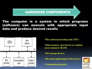
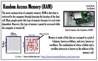
Same idea as a register file, but optimized for very many words. Small RAM: 256 4-bit words. Larger RAM: 4 million 8-bit words. Some Changes: No separate Read and Write Selects Register select lines now called ADDRESS LINES DATA IN and DATA OUT use shared wires Designed such that multiple RAM chips can be connected together to build larger memory systems (e.g., 512 MB) Random Access Memories(RAM)
1024 x 4-bit RAM Cell #0 1024 = 210 cells 10 Address Bits Cell #1 Cell #2 4 bits per cell 4 Data Bits Cell #1021 Cell #1022 Cell #1023
Typical RAM Chip Chip Select Write Enable 4 Bi-directional Data Lines (read & write) 10 Address Lines To Read: To Write:
WRITE LINES READ LINES WE Memory Buffer Register TRI-STATE LOGIC USED HERE IO0 IO3 IO2 IO1 Basic RAM Structure SELECT LINES A0 DMUX A1
1024 x 4-bit RAM will have 1024 rows, and 4 columns “Long, Thin Design” Not very practical to fabricate Long wires can make a chip run slowly Need to make the design more “square”. Practical RAM Designs
A9 Address Buffers for Row Decoders A8 Storage Matrix 64 x 64 Square Array Some Addr bits select row A7 A6 64 x 16 64 x 16 64 x 16 A5 64 x 16 A4 A3 Address Buffers for Column Decoders Some Addr bits select within row A2 Amplifiers & Mux/Demux Sense Amplifiers A1 A0 CS Data Buffers WE Tri-State Data Out I/O0 I/O1 I/O2 I/O3 A Squarer Design
We have 10 address bits, 4 data bits, and 2 control signals A conventional timing diagram will be much too big! Need some notation to represent groups of bits Bits Steady Here (May be 0 or 1) A9 … A0 Bits Can Change Here Timing Diagrams
Valid Address Access Time Read Operation WE CS Address Data Out Data Out New Notation! Center line means High-Z state (disconnected) Access Time The time it takes for new data to appear at the output
Other Timing Conventions Input Signal Output Signal Must be steady Will be steady high or low high or low High-to-low Will be changing from changes permitted high-to-low during designated interval Low-to high Will be changing from changes permitted low-to-high during designated interval Don't-Care State changing (Does not apply) Centerline represents high impedance (off) state
Memory Cycle Time Valid Address Write Timing WE CS Address Data In Input Data Data is sensed during this time
Do Activity #1 Now Explore the data sheet for a RAM chip, and answer a few questions The complete data sheets are on the course website (calendar tool, today’s date) For Qns 6 & 7, please stay consistent with the truth table on the third page of the data sheet. The circuit diagram on the first page may be a bit confusing.
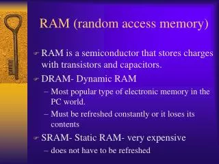
Static RAM (from first hour) Easy to understand/use: One D-type Flip Flop for each bit Fast Hard to scale up Occupies a lot of chip area Expensive Dynamic RAM Scalable: One tiny capacitor, and one transistor for each bit Slower than SRAM, but very cheap, and dense Hassles: Destructive readout Bit contents decay, so need to be refreshed periodically Types of RAM
SRAM Cell Data Data j Word Enable i Basic Idea: Try to minimize the complexity of each cell A fancy Master/Slave JK would be inappropriate here!
Single Transistor (a switch), and a capacitor memory element Word Line Bit Line Dynamic RAMs (DRAMs) To Read: assert Word Line, sense Bit Line To Write: assert Word Line, drive Bit Line Read-Out is Destructive! Extra circuits needed to write back what was read Capacitor leaks, so Storage decays in ms Refresh Cycles needed
DRAM Refresh Refresh Frequency 4096 word RAM -- refresh each word once every 4 ms Assume 120 ns memory access cycle This is one refresh cycle every 976 ns (1 in 8 DRAM accesses)! But this RAM is really organized into 64 rows This is one refresh cycle every 62.5 µs (1 in 500 DRAM accesses) Large capacity DRAMs have 256 rows, refresh once every 16 µs
Do Activity #2 Now • Due: End of Class Today. • RETAIN THE LAST PAGE(S) (#3 onwards)!! • For Next Class: • Bring Randy Katz Textbook, & TTL Data Book • Required Reading: • Sec 8.1, 8.2 of Katz • This reading is necessary for getting points in the Studio Activity!