Lecture #13
150 likes | 882 Vues
ANNOUNCEMENTS Quiz #2 next Friday (2/23) will cover the following: carrier action (drift, diffusion, R-G) continuity & minority-carrier diffusion eq’ns MS contacts (electrostatics, I-V characteristics) Review session will be held Friday 2/16 at 12:30PM

Lecture #13
E N D
Presentation Transcript
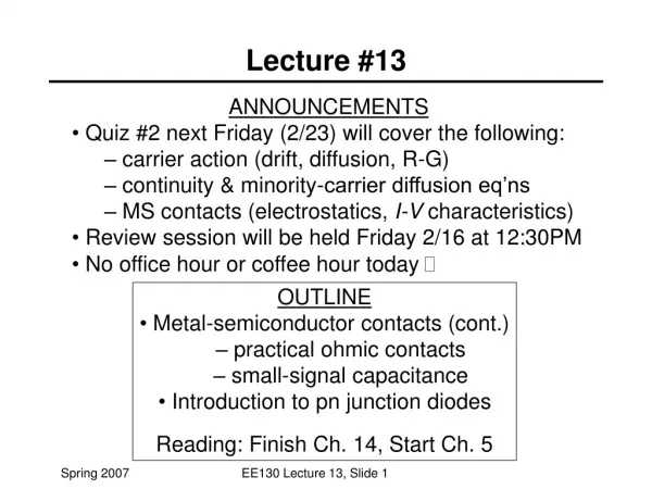
ANNOUNCEMENTS Quiz #2 next Friday (2/23) will cover the following: carrier action (drift, diffusion, R-G) continuity & minority-carrier diffusion eq’ns MS contacts (electrostatics, I-V characteristics) Review session will be held Friday 2/16 at 12:30PM No office hour or coffee hour today Lecture #13 • OUTLINE • Metal-semiconductor contacts (cont.) • practical ohmic contacts • small-signal capacitance • Introduction to pn junction diodes • Reading: Finish Ch. 14, Start Ch. 5 EE130 Lecture 13, Slide 1
Practical Ohmic Contact • In practice, most M-S contacts are rectifying • To achieve a contact which conducts easily in both directions, we dope the semiconductor very heavily W is so narrow that carriers can tunnel directly through the barrier EE130 Lecture 13, Slide 3
Band Diagram for VA0 Equilibrium Band Diagram q(Vbi-VA) qVbiFBn EFM EFM Ec, EFS Ec, EFS Ev Ev EE130 Lecture 13, Slide 5
Specific Contact Resistivity, rc • Unit: W-cm2 • rc is the resistance of a 1 cm2 contact • For a practical ohmic contact, want small FB, large ND for small contact resistance EE130 Lecture 13, Slide 6
N = dopant concentration in surface layer a = width of heavily doped surface layer • fM engineering • Impurity segregation via silicidation • Dual ( low-fM / high-fM ) silicide technology A. Kinoshita et al. (Toshiba), 2004 Symp.VLSI Technology Digest, p. 168 Approaches to Lowering fB • Image-force barrier lowering Df qfBo EF EC n+ Si metal Very high active dopant concentration desired • Band-gap reduction • strain • germanium incorporation A. Yagishita et al. (UC-Berkeley), 2003 SSDM Extended Abstracts, p. 708 M. C. Ozturk et al. (NCSU), 2002 IEDM Technical Digest, p. 375 EE130 Lecture 13, Slide 7
Voltage Drop across an Ohmic Contact • Ideally, Rcontact is very small, so little voltage is dropped across the ohmic contact, i.e.VA0V • equilibrium conditions prevail EE130 Lecture 13, Slide 8
Review: MS-Contact Charge Distribution • In a Schottky contact, charge is stored on either side of the MS junction • The applied bias VA modulates this charge EE130 Lecture 13, Slide 9
Schottky Diode: Small-Signal Capacitance • If an a.c. voltage va is applied in series with the d.c. bias VA, the charge stored in the Schottky contact will be modulated at the frequency of the a.c. voltage • displacement current will flow: EE130 Lecture 13, Slide 10
Using C-V Data to Determine FB Once Vbi and ND are known, FBn can be determined: EE130 Lecture 13, Slide 11
Summary Ec Ec EF EF Ev Ev Ec Ec EF EF Ev Ev Since it is difficult to achieve small FB, practical ohmic contacts are achieved with heavy doping: Ec EF Ec EF Ev Ev Charge storage in an MS junction small-signal capacitance: EE130 Lecture 13, Slide 12
pn Junctions – + I V I N P V Reverse bias Forward bias diode symbol EE130 Lecture 13, Slide 13
Terminology Doping Profile: EE130 Lecture 13, Slide 14
Idealized Junctions EE130 Lecture 13, Slide 15


