Understanding Op-Amp Characteristics and Applications in Signal Processing
This review explores the equivalent circuit of operational amplifiers (op-amps), focusing on typical op-amp circuits, parameters, and their behavior compared to ideal values. It elaborates on the slew rate, its calculation, and importance in amplifying signals effectively. Additionally, the functioning of various applications, such as comparators, inverting Schmitt triggers, and ADC/DAC configurations, is covered. Key points include how to measure performance and the significance of sampling periods in quantizing signals. Essential formulas and examples demonstrate practical implementation of these concepts.


Understanding Op-Amp Characteristics and Applications in Signal Processing
E N D
Presentation Transcript
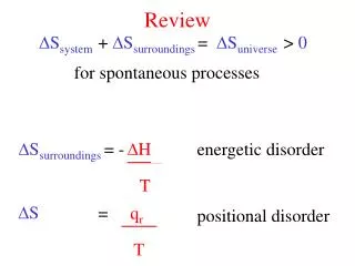
The Equivalent Circuit of the Op-Amp Typical Op-Amp circuits vd= v2 -v1 vo= Avd=A(v2 –v1) Parameters of Typical Range vs Ideal Values of the Op Amp
Slew Rate The slew rate of an op amp or any amplifier circuit is the rate of change in the output voltage caused by a step change on the input.
Slew rate calculation & formula Whereslew rate is measured in volts / second, although actual measurements are often given in v/µsf = the highest signal frequency, HzV = the maximum peak voltage of the signal. As an example, take the scenario where an op amp is required to amplify a signal with a peak amplitude of 5 volts at a frequency of 25kHz. An op amp with a slew rate of at least 2 π x 25 000 x 5 = 785,000V/s or 0.785V/µs would be required
Example: Uses a 301 op amp as a comparator. When vI < VT vO = - Vsat and vI > VT vO = + Vsat If VT ≠ 0V, the circuit is aptly called a threshold detector. If VT = 0 V, the circuit is referred to as a zero-crossing detector.
Inverting Schmitt Trigger Use a voltage divider to provide positive dc feedback for a 301 op amp. The circuit can be viewed as an inverting- type threshold detector whose threshold is controlled by the output. Since the output has two stable states, this threshold has two possible values, namely,
ADC/DAC • ADC Process • ADC Parameters • Sampling Theorem • Data Conversion Performance
Quantizing the sampled signal quantization error analogue signal quantized signal 8 levels (N =3) sampling points 3-bit ADC sampling period
DAC Equations Vout = output voltage, Vref= reference voltage, N = number of bits of precision Input_code = Vout/ Vref * 2N Vout = input_code / 2N* Vref 1 LSB = Vref / 2N
4-bit DAC example (binary weighted ladder) Input V1 is called the most significant bit ( MSB), while input V4 is the least significant bit ( LSB). Each of the three binary inputs V1, V2, V3, V4 can assume only two voltage levels: 0 or 1V.
Let Rf = 10 kΩ, R1 = 10 kΩ, R2= 20 kΩ, R3= 40 kΩ, and R4= 80 kΩ. Obtain the analog output for binary inputs [ 0000], [ 0001], [ 0010], . . . , [ 1111]. This is an inverting summing amplifier. The output is related to the inputs as shown below: -VO = V1 + 0.5V2 + 0.25V3 + 0.125V4 A digital input [ V1V2V3V4] = [ 0000] = 0V = -Vo [ V1V2V3V4] = [ 0001] = 0.125V4 = 0.125 x 1V = 0.125V = -Vo [ V1V2V3V4] = [ 0010] = 0.25V3 = 0.25 x 1V = 0.25V = -Vo [ V1V2V3V4] = [ 0011] = 0.25V3 + 0.125V4 = 0.25 + 0.125 = 0.375V = -Vo . . . [ V1V2V3V4] = [ 1110] = V1 + 0.5V2 + 0.25V3 + 0V4= 1. 75V = -Vo [ V1V2V3V4] = [ 1111] = V1 + 0.5V2 + 0.25V3 + 0.125V4 = 1.875V = -Vo
ADC Equations Vin = input voltage, Vref+ = ref voltage, Vref-= 0 V, (Note: Vref= VFS) N = number of bits of precision output_code = Vin / Vref * 2N Vin = output_code / 2N* Vref 1 LSB = Vref / 2N
Comparing types of ADCs Flash ADC Successive Approximation Converter
Vin= 3.4V Vappr Successive-approximation ADC Binary search for a 3-bit ADC Vref: 5V full scale value D2 D1 D0 4.375V 1 1 1 3.750V 1 1 0 3.125V 1 0 1 2.500V 1 0 0 0 1 1 1.875V 0 1 0 1.250V 0 0 1 0.625V 0.000V 0 0 0 clock cycle 2 D1 = 0 [Vin < Vappr] clock cycle 1 D2 = 1 [Vin > Vappr] clock cycle 3 D0 = 1 [Vin > Vappr] 3.4 > (5 + 0)/2 = 2.5 Bit 2 = 1 3.4 < (5 + 2.5)/2 = 3.75 Bit 1 = 0 3.4 > (3.75 + 2.5)/2 = 3.125 Bit 0 = 1
3-bit flash ADC Flash ADC
Successive Approximation Converter Speed: High Cost: High Accuracy: High but limited
DC-DC Converters • Linear Regulator • How does it work? • Efficiency • Switching Mode Regulator • Type of switching mode regulator • How does Buck converter work? • Efficiency
References: Fundamentals of Electric Circuits, 5th Edition Alexander, Charles; Sadiku, Matthew TI MSP-EXP430F5529 LaunchPad User’s Guide TI TSP62237 Specs