Chapter 3 Materials and Basic Processes
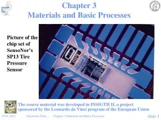
Chapter 3 Materials and Basic Processes. Picture of the chip set of SensoNor’s SP13 Tire Pressure Sensor. The course material was developed in INSIGTH II, a project sponsored by the Leonardo da Vinci program of the European Union. Materials: Metals.

Chapter 3 Materials and Basic Processes
E N D
Presentation Transcript
Chapter 3Materials and Basic Processes Picture of the chip set of SensoNor’s SP13 Tire Pressure Sensor The course material was developed in INSIGTH II, a project sponsored by the Leonardo da Vinci program of the European Union Electronic Pack….. Chapter 3 Materials and Basic Processes
Materials: Metals • Right choice, right use and compatibility of materials is the key to good packaging and optimal properties. • Elemental metals: • High electrical conductivity • High thermal conductivity • Higher thermal coefficient of expansion (TCE) than semiconductors and most ceramics • Alloys: taylored to many uses: • Poorer electrical and thermal conductivity than elements • Taylored TCE • Lower melting point Electronic Pack….. Chapter 3 Materials and Basic Processes
Metals, continued • (Table 3.1) Electronic Pack….. Chapter 3 Materials and Basic Processes
Metal Alloys • Alloys have poorer conductivity, both electrical and thermal. • Fig. 3.1: Phase diagram for Sn/Pb. The eutectic mixture 63%/37% has a melting point of 183°C. Electronic Pack….. Chapter 3 Materials and Basic Processes
Insulators • (Fig 3.1b) Electronic Pack….. Chapter 3 Materials and Basic Processes
Semiconductors, Si and GaAs • High thermal conductivity • Electrical conductivity spans many orders of magnitude, depending on doping • Very low TCE • "Machinable" by anisotropic etching (Si) • Excellent protective oxide (Si) Electronic Pack….. Chapter 3 Materials and Basic Processes
Ceramics • Inorganic, non-metallic materials (Defined by what they not are) • Man made/Synthetic made: Made by powder, compressing or tape casting, and high temperature treatment (600-1800oC) • Generally chemically and thermally very stable • Generally good electrical insulators • Some ceramics are very good thermal conductors Electronic Pack….. Chapter 3 Materials and Basic Processes
Ceramics, continued Electronic Pack….. Chapter 3 Materials and Basic Processes
Ceramics, continued • Dielectric loss: • tan d = (1/R)/wC = 1/Q • e = eo(k´ - jk") • tan d = k"/k´. • Main uses: • Substrates for hybrid circuits, component packages, SMD resistors • Multilayer capacitors • Future: Superconductors ? Electronic Pack….. Chapter 3 Materials and Basic Processes
Materials • Fig 3.1.d Electronic Pack….. Chapter 3 Materials and Basic Processes
Ceramics, continued Electronic Pack….. Chapter 3 Materials and Basic Processes
Ceramics, continued Electronic Pack….. Chapter 3 Materials and Basic Processes
Glasses: • Glasses are amorphous, supercooled liquids • Uses: • Matrix for thick film pastes • Hermetic seals • Substrates, together with ceramics Electronic Pack….. Chapter 3 Materials and Basic Processes
Plastics • Organic, synthetic polymer materials with numerous uses in electronics Electronic Pack….. Chapter 3 Materials and Basic Processes
Plastics, continued • Composition, properties: • Monomers derived from benzene Electronic Pack….. Chapter 3 Materials and Basic Processes
Plastics, continued Electronic Pack….. Chapter 3 Materials and Basic Processes
Plastics, continued • Requirements: • High electrical resistivity, high breakdown field, low dielectric losses, low dielectric constant • Thermal and mechanical stability • Thermal expansion compatible with Si and metals • High mechanical strength/softness and flexibility • Chemical resistance • Good adhesion to other materials • Ease of processing • Low water absorption, small changes of the properties during the effect of moisture. Electronic Pack….. Chapter 3 Materials and Basic Processes
Plastics, continued • Composition, properties: • Linear, branched or crosslinked Electronic Pack….. Chapter 3 Materials and Basic Processes
Plastics, continued • Thermoplastic or thermosetting Electronic Pack….. Chapter 3 Materials and Basic Processes
Plastics, continued • Polymerization: A-, B-, C-stages. • High electrical resistivity , low dielectric constant r, low loss factor tan , high breakdown field Ecrit • Poor thermal conductors • Visco-elastic • Fig 3.7: The structural unit of certain monomers/polymers. Electronic Pack….. Chapter 3 Materials and Basic Processes
Plastics, continued • "Glass transition": change from glass-like to rubber - like Electronic Pack….. Chapter 3 Materials and Basic Processes
Plastic Materials: • Epoxy • Phenolic • Polyimide • Teflon • Polyester • Silicone • Polyurethane • Parylene • Acrylic • Polysulphone, polyethersulphone, polyetherimide Electronic Pack….. Chapter 3 Materials and Basic Processes
Plastics, continued • Fig. 3.9: a):The epoxide group, which is the building block in epoxy, b) - e): Starting materials for epoxy:b): Bisphenol A, which constitutes most of the starting material. The H-atoms in the places X are often replaced with Br to reduce the flammability; c): Epoxy novolac; d): The hardener dicyandiamide; e): The catalyst. Electronic Pack….. Chapter 3 Materials and Basic Processes
Plastics, continued Electronic Pack….. Chapter 3 Materials and Basic Processes
Basic Processes • Description of some of the basic processes used in microelectronics, microsystems and electronic packaging. Electronic Pack….. Chapter 3 Materials and Basic Processes
Photolithography • Fig. 3.10:The steps in photolithographic transfer of patterns and the subsequent etching of metal films with negative photoresist. • If positive resist is used, it is the illuminated part of the photoresist, which is removed during the development. • Positive resist most used today because of better accuracy Electronic Pack….. Chapter 3 Materials and Basic Processes
Photolithography • Colour graph downloaded from Wikipedia (1602-2012: http://en.wikipedia.org/wiki/Photolithography • Self test: Explain the difference between positive and negative resist. Electronic Pack….. Chapter 3 Materials and Basic Processes
Photolithography, cont • Also, please observe the concept of straight polarity masks and reverse polarity masks: • Straight polarity:In layers with straight polarity, a positive image of the layout will be transferred onto the process layer. In other words, draw the objects that need to be covered with photo-resist after development. • Openings: Mask pattern is repeated on the substrate for additive films etc., like metal patterns. (Assuming positive resist is used) • Reverse polarity:In layers with reverse polarity, draw the areas where photo-resist should be removed. The actual mask will be the negative image of the layout. • Mask pattern is oppositely repeated on the substrate for additive films etc., like openings in oxide for later difussion of dopants. (Assuming positive resist is used) Electronic Pack….. Chapter 3 Materials and Basic Processes
Screen Printing and Stencil Printing • Fig. 3.11: Screen printing: a) and b): Printing process, c) and d): Details of thescreen Electronic Pack….. Chapter 3 Materials and Basic Processes
Etching • Wet, chemical etching • "Dry" plasma- or reactive ion etching • Examples, wet etching:Copper:FeCl3 + Cu -> FeCl2 + CuClIn addition:FeCl3 + CuCl -> FeCl2 + CuCl2Need organic etch resist, not good with PbSn.Gold:KI + I2 -> KI3 + KI (surplus)3 KI3 + 2 Au -> 2 KAuI4 + KI Electronic Pack….. Chapter 3 Materials and Basic Processes
Plating • Electrolytic plating: • Electric current of ions in electrolyte. External circuit needed. All separate parts of area to be plated must be electrically contacted to external circuit.Example: Cu in CuSO4 /H2SO4 Reaction at anode (Cu supply): Cu -> Cu2+ + 2e- Reaction at catode (substrate): Cu2+ + 2e- -> Cu Electronic Pack….. Chapter 3 Materials and Basic Processes
Plating, continued • Chemical plating: • Takes place without external current • Needed when insulating surfacec are to be plated • Often preceeds electrolytic plating, to make all needed areas electrically conductive • Complex processes of "sensitizing", "activation" and plating Electronic Pack….. Chapter 3 Materials and Basic Processes
Vacuum Deposition and Sputtering • Vacuum evaporation: • Chamber evacuated toless than 10-6 Torr • Resistance heating • Metal evaporation Electronic Pack….. Chapter 3 Materials and Basic Processes
Other Methods for Deposition of Conducting or Insulating Films • DC Sputtering (Fig. 3.13.a) Electronic Pack….. Chapter 3 Materials and Basic Processes
Deposition, continued • Radio Frequency AC Sputtering (Fig.3.13.b) Electronic Pack….. Chapter 3 Materials and Basic Processes
Methods for Electrical and Mechanical Contact • Soldering • Wetting: (Fig. 3.14) Young´s eq.: gls + gl cos Q = gs Electronic Pack….. Chapter 3 Materials and Basic Processes
Leadless soldering • Leadless soldering replacing lead-based solder due health hazards and environmental issues
Soldering, continued • Most common solder alloy: 63 % Sn / 37 % Pb (eutectic)Melting point 183 oC Electronic Pack….. Chapter 3 Materials and Basic Processes
Soldering, continued • Fatigue: Coffin-Mansons formula:N0.5 x gp = constantwhere N is number of stress cycles, and gp is the relative deformation amplitude, meaning that both number of cycles and stress level determine lifetime • Useful adition : 2 % Ag (Surface mount), to reduce leaching (dissolution of the termination metal that leads to deterioration of mechanical and electrical properties) • Harmful contaminant: Au, will increase brittleness because of AuSn intermetallics Electronic Pack….. Chapter 3 Materials and Basic Processes
Soldering, continued • Fig.3.15: Behaviour of solder metal at different temperatures, schematically. [W. Engelmaier]. Electronic Pack….. Chapter 3 Materials and Basic Processes
Soldering, continued • Fig. 3.16: Solder joint fatigue in surface mounted assemblies is often caused by power cycling. Electronic Pack….. Chapter 3 Materials and Basic Processes
Soldering, continued • Fig. 3.17: Experimental data for fatigue in Sn/Pb solder fillet by cyclical mechanical stress. High temperature and low cycling frequency gives the fastest failure, because the grain structure relaxes most and is damaged Electronic Pack….. Chapter 3 Materials and Basic Processes
Soldering, continued • Fig. 3.18. a) Left: Dissolution rate of Ag in solder metal, and in solder metal with 2 % Ag, as function of temperatureb) Right: Dissolution rate of various metals in solder alloy Electronic Pack….. Chapter 3 Materials and Basic Processes
Soldering, continued Electronic Pack….. Chapter 3 Materials and Basic Processes
Soldering, continued • Flux and cleaning • Purpose of flux: • Dissolve and remove oxides etc. • Protect surface • Improve wetting • Categories: • Soluble in organic liquids • Water soluble • Types: • Organic resin fluxes ("rosin") • Organic non resin based fluxes • Inorganic fluxes Electronic Pack….. Chapter 3 Materials and Basic Processes
Soldering: Flux and cleaning • Fig. 3.19: Time for solder alloy to wet a pure Cu surface, depending on the activation of the solder flux. The degree of activation is given by the concentration of Cl- ions in the flux (temperature: 230 °C) Electronic Pack….. Chapter 3 Materials and Basic Processes
Soldering: Flux and Cleaning • Designations: • R (Rosin, non-activated): No clorine added. • RMA (Rosin mildly activated): < 0.5 % Cl • RA (Rosin, activated): > 0.5 % Cl • Cleaning • Freon (TCTFE) now forbidden. Replaced by alcohol etc. • Trend: No cleaning Electronic Pack….. Chapter 3 Materials and Basic Processes
Gluing • Purposes: • Mechanical assembly • Electrical contact • Thermal contact • Materials: polymers: • Epoxy, acrylic, phenolic, polyimide • Metal particles for electrical conductivity: r = 1 - 10 x 10 -6 ohm m • Metal or ceramic particles for thermal conductivity: K ≈ 1 - 3 W /m x oC Electronic Pack….. Chapter 3 Materials and Basic Processes
Gluing, continued • Fig. 3.20: Thermal conductivity of epoxy adhesive with various amounts of Ag [3.16 a)]. The concentration is in volume % Ag. (23 vol. % corresponds to approximately 80 weight %). Electronic Pack….. Chapter 3 Materials and Basic Processes
Gluing, continued • Fig. 3.21: The thermal resistance from the electronically active part, on top of the Si chip (¨junction¨) through a bonding layer of glue or soft solder and a thin alumina ceramic layer covered with Cu to heat sink. The samples with chips bonded by gluing, C and A, have approximately twice as high total thermal resistance as those which are soft soldered, D and B. Electronic Pack….. Chapter 3 Materials and Basic Processes