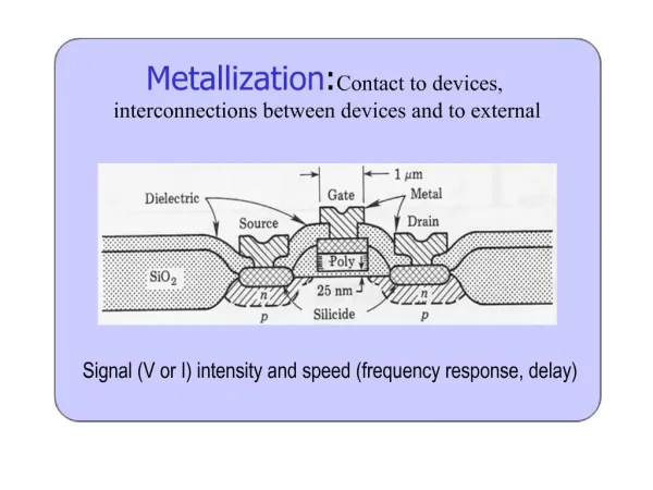
Metallization
Metallization. ECE/ChE 4752: Microelectronics Processing Laboratory. Gary S. May February 26, 2004. Outline. Introduction Physical Vapor Deposition Chemical Vapor Deposition Aluminum Metallization Copper Metallization. Basics. Goal : form low-resistance interconnections Types :

Metallization
E N D
Presentation Transcript
Metallization ECE/ChE 4752: Microelectronics Processing Laboratory Gary S. May February 26, 2004
Outline • Introduction • Physical Vapor Deposition • Chemical Vapor Deposition • Aluminum Metallization • Copper Metallization
Basics • Goal: form low-resistance interconnections • Types: • Physical vapor deposition (PVD) – evaporation or sputtering • Chemical vapor deposition (CVD) – involves a chemical reaction
Uses • MOS gates • Contacts • Interconnect
Requirements • Uniformity and conformal coating • High conductivity • High reliability
Outline • Introduction • Physical Vapor Deposition • Chemical Vapor Deposition • Aluminum Metallization • Copper Metallization
Basics • Also called “evaporation” • Goal: evaporate metal; condense on wafer surface • Procedure: • Convert metal from solid to vapor phase (melt + evaporate or direct sublimation) • Transport gaseous material to substrate • Condense gaseous material on substrate
Evaporation Equipment • Conditions: • High temperature • Low pressure (10-6 – 10-7 torr)
Achieving Low Pressure • Evaporation chamber must be “pumped down” where: P(t) = chamber pressure at time t, P0 = initial pressure, S = pumping speed, Q = rate of outgassing, V = volume of chamber • Pumping apparatus has 2-stages: 1) roughing pump: atm -> 10-3 torr 2) diffusion pump: 10-3 -> 10-6 torr
Kinetic Gas Theory • Ideal gas law: PV = NavkT where: k = Boltzmann constant, Nav = Avogadro’s # (6.02 x 10²³ molecules/mole), P = pressure, V = volume, T = temperature • Concentration of gas molecules given by: n = Nav/V = P/kT
Deposition Rate • Impingement rate of gas molecules hitting surface: where: P = pressure (N/m2), M = molecular weight (g/mole), T = temperature (oK) • Time to form one monolayer t = Ns/F where: Ns = # molecules/cm2 in the layer molecules/cm2-s
Geometric Variation • Deposition rate has radial dependence: where: D0 = deposition rate at center of wafer
Surface Profiometry • Used to measure deposited film thickness • Precision = 2 Å
Limitations of Evaporation 1. Low melting point of Al 2. Difficult to achieve very large or small thicknesses (typical range = 0.05 - 5 mm) • Alternative = sputtering • Advantages: • Better step coverage • Less radiation damage then e-beam • Better at producing layers of compound materials
Sputtering • Source of ions is accelerated toward the target and impinges on its surface
Outline • Introduction • Physical Vapor Deposition • Chemical Vapor Deposition • Aluminum Metallization • Copper Metallization
Advantages • Conformal coatings • Good step coverage • Can coat a large number of wafers at a time • Lower electrical resistivity films than PVD • Allows refractory metal (like W) deposition
Outline • Introduction • Physical Vapor Deposition • Chemical Vapor Deposition • Aluminum Metallization • Copper Metallization
Properties • Can be deposited by PVD or CVD • Al and its alloys have low resistivity (2.7 mW-cm for Al and up to 3.5 mW-cm for alloys) • Adheres well to silicon dioxide • Use with shallow junctions can create problems, such as spiking or eletromigration
Eutectic Characteristics • Addition of either component lowers Al-Si system melting point below that of either metal (660 °C for Al and 1412 °C for Si) • Eutectic temperature (577 °C) corresponds to 11.3% Al and 88.7% Si. • Al deposition the temperature must be less than 577 °C.
Solubility of Al in Si • Si dissolves into Al during annealing • After time t, Si diffuses a distance of (Dt)0.5 along Al line from the edge of the contact • Depth to which Si is consumed given by where: r = density, S = solubility of Si, and A = ZL
Junction Spiking • Dissolution of Si take place at only a few points, where spikes are formed • One way to minimize spiking is to add Si to the Al by co-evaporation. Another method is to introduce a barrier metal (such as TiN) between the Al and Si
Electromigration • High current densities can cause the transport of mass in metals • Occurs by transfer of momentum from electrons to positive metal ions • Metal ions in some regions pile up and voids form in other regions • Pileup can short-circuit adjacent conductors, whereas voids can result in open circuits
Mean Time to Failure • MTF due to electromigration is be related to the current density (J) and activation energy by • Experimentally, Ea = 0.5 eV for aluminum • Electromigration resistance of Al can be increased by alloying with Cu (e.g., A1 with 0.5% Cu), encapsulating the conductor in a dielectric, or incorporating oxygen during deposition.
Outline • Introduction • Physical Vapor Deposition • Chemical Vapor Deposition • Aluminum Metallization • Copper Metallization
Motivation • High conductivity wiring and low–dielectric-constant insulators are required to lower RC time delay of interconnect. • Copper has higher conductivity and electromigration resistance than Al. • Cu can be deposited by PVD or CVD, • Downside: • Cu tends to corrode under standard processing conditions • Not amenable to dry etching • Poor adhesion to SiO2
Damascene Technology • Trenches for metal lines defined and etched in interlayer dielectric (ILD) • Metal deposition of TaN/Cu (TaN serves as a diffusion barrier to prevent Cu from penetrating the dielectric) • Excess Cu on the surface is removed to obtain a planar structure.
Chemical Mechanical Polishing • Allows global planarization over large and small structures • Advantages: • Reduced defect density • No plasma damage • Consists of moving sample surface against pad that carries slurry between the sample surface and the pad.