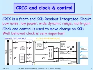
CRIC and clock & control
90 likes | 106 Vues
CRIC is a front-end CCD Readout Integrated Circuit designed for low noise, low power, and wide dynamic range. It includes clock and control functions for CCD charge movement. The well-behaved clock is crucial for high-quality imaging. This IC meets the requirements of low noise, large dynamic range, high readout frequency, radiation tolerance, low power, and operation at different temperatures. CRIC is compact, robust, and space qualified, making it suitable for various applications.

CRIC and clock & control
E N D
Presentation Transcript
CRIC and clock & control CRIC is a front-end CCD Readout Integrated Circuit Low noise, low power, wide dynamic range, multi-gain Clock and control is used to move charge on CCD Well behaved clock is very important William Wester, Fermilab, Internal CTIO Camera meeting
Requirements • Low noise:Photometry: CCD + electronic noise 4e rms (14mV)Spectrograph: CCD + electronic noise 2e rms (7mV) • Large dynamic range:96dB from noise floor to 130ke well depth (16-bit) • Readout frequency: 100 kHz & 50kHz • Radiation tolerant 10 kRad ionization (well shielded) • Low power 200mJ/image/channel => 10mW/channel • Operation at 140K and 300KAllow normal operation at 140K and chip testing at room temperature • Compact • Robust, space qualified Spec’s exceed sky noise that dominate DECam See JP Walder presentation at NSS 2003! William Wester, Fermilab, Internal CTIO Camera meeting
Timing: RG Thermal and 1/f noise of the output transistor SW Thermal noise of the output resistor Output signal Reset level Frozen noise charge, with a variance of kTC, stored in Cfd just after reset. Video + reset level Thermal and 1/f noise kTC noise Thermal noise Noise on the CCD Sensor • Correlated double sampling removes reset level and the kTC noise and reduces 1/f noise. • Integration: reduces the thermal noise. William Wester, Fermilab, Internal CTIO Camera meeting
Single CRIC Channel CCD conversion gain: 3.5mV/e C Switch matrix Out+ R Vn R1 R2 A3 Vout R1 Vn R2 - R - A1 A2 (CDS) + Out- + Vn C CCD noise source Out (t=4ms) t t time Reset integration Signal integration Real integration during 2t. Good rejection of the CCD thermal noise. William Wester, Fermilab, Internal CTIO Camera meeting
Multi-ranging is built-in Poisson electronic noise William Wester, Fermilab, Internal CTIO Camera meeting
Simulation results Full scale signal simulation at 100kHz readout rate Gain 2 Indicator bit Gain 1 Indicator bit Output signal William Wester, Fermilab, Internal CTIO Camera meeting
Actual device Fabricated test chip (no-ADC) Four channels and test structures Good results with testing so far Next version submitted in March has ADC Good linearity and noise William Wester, Fermilab, Internal CTIO Camera meeting
Comments CRIC chip is actively being developed for use with SNAP CCDs I personally think it’s a no-brainer to use this device for analog-to-digital on the focal plane Power is low and plans for packaging have a CRIC board Clock and control is open as to what’s on the focal plane and what’s not William Wester, Fermilab, Internal CTIO Camera meeting
Cost and schedule exists $1K/chip ~$100K H. Von der Lippe Other cost savings possibilities exist William Wester, Fermilab, Internal CTIO Camera meeting