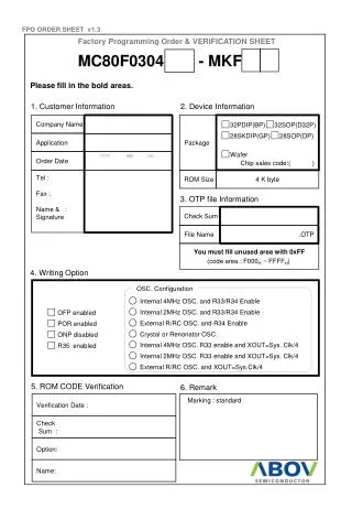
Factory Programming Order & Verification Sheet
Fill in bold areas for Customer and Device Information, OTP file, Writing Options, ROM CODE Verif., and Remarks.

Factory Programming Order & Verification Sheet
E N D
Presentation Transcript
FPO ORDER SHEET v1.3 Factory Programming Order & VERIFICATION SHEET MC80F0304 - MKF Please fill in the bold areas. 1. Customer Information 2. Device Information Company Name Package □32PDIP(BP)□32SOP(D32P) □28SKDIP(GP)□28SOP(DP) □Wafer Chip sales code:( ) Application Order Date YYYY MM DD Tel : Fax : Name & : Signature ROM Size 4 K byte 3. OTP file Information Check Sum File Name .OTP You must fill unused area with 0xFF (code area : F000H ~ FFFFH) 4. Writing Option □ OFP enabled □ POR enabled □ ONP disabled □ R35 enabled ○ Internal 4MHz OSC. and R33/R34 Enable ○ Internal 2MHz OSC. and R33/R34 Enable ○ External R/RC OSC. and R34 Enable ○ Crystal or Renonator OSC. ○ Internal 4MHz OSC. R33 enable and XOUT=Sys. Clk/4 ○ Internal 2MHz OSC. R33 enable and XOUT=Sys. Clk/4 ○ External R/RC OSC. and XOUT=Sys.Clk/4 OSC. Configuration 5. ROM CODE Verification 6. Remark Verification Date : Marking : standard Check Sum : Option: Name:
FPO ORDER SHEET v1.3 Factory Programming Order & VERIFICATION SHEET MC80F0308 - MKF Please fill in the bold areas. 1. Customer Information 2. Device Information Company Name Package □32PDIP(BP)□32SOP(D32P) □28SKDIP(GP)□28SOP(DP) □Wafer Chip sales code:( ) Application Order Date YYYY MM DD Tel : Fax : Name & : Signature ROM Size 8 K byte 3. OTP file Information Check Sum File Name .OTP You must fill unused area with 0xFF (code area : E000H ~ FFFFH) 4. Writing Option □ OFP enabled □ POR enabled □ ONP disabled □ R35 enabled ○ Internal 4MHz OSC. and R33/R34 Enable ○ Internal 2MHz OSC. and R33/R34 Enable ○ External R/RC OSC. and R34 Enable ○ Crystal or Renonator OSC. ○ Internal 4MHz OSC. R33 enable and XOUT=Sys. Clk/4 ○ Internal 2MHz OSC. R33 enable and XOUT=Sys. Clk/4 ○ External R/RC OSC. and XOUT=Sys.Clk/4 OSC. Configuration 5. ROM CODE Verification 6. Remark Verification Date : Marking : standard Check Sum : Option: Name:
FPO ORDER SHEET v1.3 Factory Programming Order & VERIFICATION SHEET MC80F0316 - MKF Please fill in the bold areas. 1. Customer Information 2. Device Information Company Name Package □32PDIP(BP)□32SOP(D32P) □28SKDIP(GP)□28SOP(DP) □Wafer Chip sales code:( ) Application Order Date YYYY MM DD Tel : Fax : Name & : Signature ROM Size 16 K byte 3. OTP file Information Check Sum File Name .OTP You must fill unused area with 0xFF (code area : C000H ~ FFFFH) 4. Writing Option □ OFP enabled □ POR enabled □ ONP disabled □ R35 enabled ○ Internal 4MHz OSC. and R33/R34 Enable ○ Internal 2MHz OSC. and R33/R34 Enable ○ External R/RC OSC. and R34 Enable ○ Crystal or Renonator OSC. ○ Internal 4MHz OSC. R33 enable and XOUT=Sys. Clk/4 ○ Internal 2MHz OSC. R33 enable and XOUT=Sys. Clk/4 ○ External R/RC OSC. and XOUT=Sys.Clk/4 OSC. Configuration 5. ROM CODE Verification 6. Remark Verification Date : Marking : standard Check Sum : Option: Name: