IC Processing
IC Processing. Initial Steps: Forming an active region. Photoresist is chemically removed in acid, or stripped in an O 2 plasma. After stripping photoresist, field oxide is grown. Field oxide provides insulation between adjacent junctions.

IC Processing
E N D
Presentation Transcript
Initial Steps: Forming an active region Photoresist is chemically removed in acid, or stripped in an O2 plasma After stripping photoresist, field oxide is grown. Field oxide provides insulation between adjacent junctions Si3N4 is etched away using an F-plasma: Si3dN4 + 12F → 3SiF4 + 2N2 Or removed in hot phosphoric acid
N and P wells are formed Photoresist mask is applied, and active ions implanted by ion bombardment. Typically, 150-200 keV accelerating energy After implantation, ions are diffused into substrate to form wells
After well formation, additional N and P layers are formed in respective N and P wells, then a layer of polysilicon is deposited. Polysilicon is electrically conductive and used for gate voltage connections.
Insulating layers of SiO2 are grown around the gate, followed by N or P bombardment for form the NMOS or PMOS source and drain regions. After forming gate, source and drain regions, Ti film is deposited by sputtering to act as electrical interconnect
Ti is reacted with Nw to form TiSi2 where it contacts silicon (black regions) or TiN elsewhere. Then, it is coated with photoresist and etched, followed by deposit of another insulating SiO2 layer. Another coat of photoresist followed by etching exposes gates for connections
A barrier region of TiN is applied, followed by thin-film application of W, which undergoes CMP to provide a flat surface with exposed contacts Finally, aluminum is sputtered on wafer, masked and plasma etched. Additional interconnect layers may be added the same way.
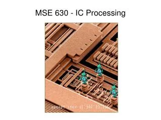
SEM photograph of interconnects formed in an integrated circuit. Conductive metals are carefully chosen to provide right conductivity (or resistivity) and dielectric properties
K1 ~ 0.6-0.8 and K2 ~ 0.5. NA is the numerical aperture number, NA=n*sin(a) where n=1 and a is the angle formed by the point light source and the aperture width
Example Estimate the resolution and depth of focus of an excimer laser stepper using KrF light source (l = 248 nm) and NA=0.6 Assume k1 = 0.75 and k2 = 0.5. Solution: R = k1*l/NA = 0.75(0.248/0.6) = 0.31 nm DOF = ± k2*l/NA2 = ±0.5(0.248/(0.6)2) = ±0.34 mm
Shrinking device size drives need for finer replication methods:
Diffusion is not constant across cross section, and continues with every subsequent high-temperature step; hence, we use charts as below to calculate surface concentrations, Cs, from average conductivity,
Effective diffusion-time, (Dt)eff, is the sum of the diffusivity and time at each step: (Dt)eff= D1t1+D1t2(D2/D1)=D1t1+D2t2 Effective diffusivity is: DAeff=Do+D-(n/ni)+D=)n/ni)2 for N-type DeffA=Do+D+(p/ni)+D++(p/ni)2 for P-type Values are tabulated, as in table 7.5
Example Figure 7-17 Dopant surface concentration vs. effective conductivity for various substrate concentrations, CB

