Download
1 / 27
380 likes | 735 Vues
CAD Tools for Circuit Design Electronics Unit – Lecture 5. Schematic Diagram Drawing Etched Circuit Board Layout Circuit Simulation. Schematic Capture. Many CAD packages available for design, simulation, and layout. Will use ExpressPCB suite for example

E N D
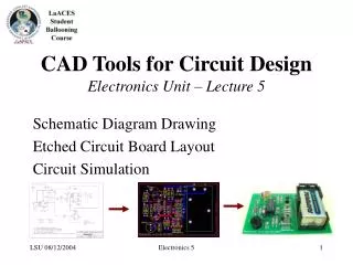
CAD Tools for Circuit DesignElectronics Unit – Lecture 5 Schematic Diagram Drawing Etched Circuit Board Layout Circuit Simulation Electronics 5
Schematic Capture Many CAD packages available for design, simulation, and layout. Will use ExpressPCB suite for example Extensive library of standard components Custom components can be created Does not include a simulation function Electronics 5
ExpressSCH Main screen User’s manual and Quick Start Guide Component selection tools After startup, maximize the window, choose View menu, then Zoom To Fit Pick out a library component, for example a 555 timer chip. View Help screens as needed Electronics 5
Choosing Components from Menu Click on the desired component. A cursor will appear. Position the cursor and click, the symbol will be added to the drawing. Click again to duplicate the symbol. Electronics 5
Placing Components Zoom tool Click and drag to move the component around the drawing Use the Zoom tool to get a closer look. Electronics 5
Using the Component Manager Choose Component menu, then select Component and symbol manager Component menu Electronics 5
Using the Component Manager Choose Component menu, then select Component and symbol manager. Select a component, then click Insert into schematic. Electronics 5
Component Properties Right click on a component, then open the Set component properties window. Part ID and value can be set, as well as other properties. Electronics 5
A closer look at components Note U1 has numbered pins, Q1 does not. Pin numbers may be hidden. Click on a pin to view the pin number. Pin number display Electronics 5
Adding a Wire Connection Wire tool Left click at the start and at each desired corner. Right click when done. Electronics 5
Power and Ground NOT a connection Library components include symbols for power sources and ground (common) connections. IS a connection Electronics 5
Creating Custom Components Components are created as groups of: Rectangles Lines Arcs Pins Electronics 5
Custom Components line arc Draw the component. Assign pin numbers and names. Select the component. Access the Component menu and choose Group to make component. Assign component properties, such a ID and type. pin rectangle Electronics 5
Component Properties Afterwards, choose Save custom component from Component menu Electronics 5
Ready for Use Connect the custom component into the circuit. If desired, use Component manager to add the component to your Favorites list Electronics 5
Circuit Board Layout After drawing the circuit with ExpressSCH, use ExpressPCB to design a pattern for an etched circuit board. Schematic can be linked to the board layout to aid in placing components and routing interconnections. Correct pin numbering will be essential. Electronics 5
Boards Have Three Layers Top Layer – an etched copper pattern Bottom Layer – an etched copper pattern Silk Screen – an inked pictorial pattern Top and bottom layers may include Traces – a copper path interconnecting two or more points Vias – a connection between the top and bottom layers, with a continuous plated copper path existing through the hole Pads – a point where a component lead will be connected most pads exist on both top and bottom layers and incorporate a through-hole, thus also serve as a via. Electronics 5
Component patterns are saved arrays of pads which must match the shape of a physical component. It usually includes a silkscreen outline of the component. Custom components can be created, just as in ExpressSCH. place a pad or via layer selection place a component place a trace Electronics 5
Pad Characteristics Pad inner diameter sets the size of the through-hole. Must be large enough to accept the wire lead of the component. Outer diameter controls how much solder-accepting surface is available. OD = 0.062” and ID = 0.029” is a common pad for small components Electronics 5
Trace Characteristics Trace width determines the amount of current the trace can carry without excessive voltage drop or heating. See Design Tips under the ExpressPCB Help menu for suggested trace widths. Examples: a 0.025” trace can carry up to about 1 amp a 0.050 trace is good for up to about 2 amps Electronics 5
A Very Simple Design Example Design a one transistor amplifier, with capacitively coupled input and output. A protection diode should be used to protect the transistor from reverse polarity. Electronics 5
First Draw the Schematic Diagram After all components are named and labeled, select Check schematic for netlist errors from the File menu. Leave this window open, then open an ExpressPCB window. Electronics 5
Now Place All Components Don’t worry about connecting them with traces yet. Name each component to match the name on the schematic. Select Link schematic to PCB from File menu. Electronics 5
Connect Components Together Use the Highlight net connections tool to identify which pads should be joined with traces. Blue dots indicate points that should be connected, according to the linked schematic Highlight net connections tool Electronics 5
Connect Components Together Re-arrange the components for the most efficient interconnects. Highlight net connections tool Electronics 5
Connect Components Together Re-arrange the components for the most efficient interconnects. Then add the traces. Use the bottom side as much as possible. This example uses much too much space. It’s just an illustration. Highlight net connections tool Electronics 5
Activity E5 Design a simple power supply using a three terminal regulator integrated circuit. Draw the schematic. Lay out a circuit board. Electronics 5