Emitter Follower Amplifier Analysis Techniques
210 likes | 280 Vues
Learn how to analyze Emitter Follower Amplifier using various techniques, calculate parameters like IC, IB, VCE, and determine poles and zeros frequencies for both low and high frequency responses.

Emitter Follower Amplifier Analysis Techniques
E N D
Presentation Transcript
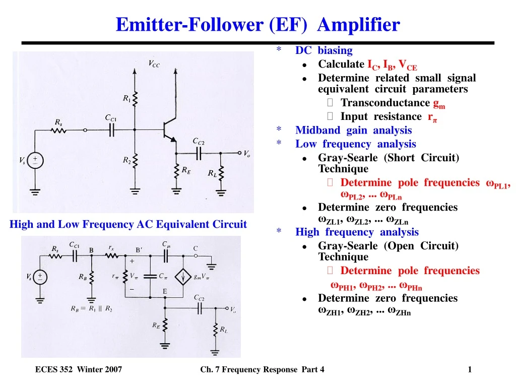
Emitter-Follower (EF) Amplifier • DC biasing • Calculate IC, IB, VCE • Determine related small signal equivalent circuit parameters • Transconductance gm • Input resistance rπ • Midband gain analysis • Low frequency analysis • Gray-Searle (Short Circuit) Technique • Determine pole frequencies ωPL1, ωPL2, ... ωPLn • Determine zero frequencies ωZL1, ωZL2, ... ωZLn • High frequency analysis • Gray-Searle (Open Circuit) Technique • Determine pole frequencies ωPH1, ωPH2, ... ωPHn • Determine zero frequencies ωZH1, ωZH2, ... ωZHn High and Low Frequency AC Equivalent Circuit Ch. 7 Frequency Response Part 4
EF Amplifier - DC Analysis (Nearly the Same as CE Amplifier) • GIVEN: Transistor parameters: • Current gain β= 200 • Base resistance rx = 65 Ω • Base-emitter voltage VBE,active = 0.7 V • Resistors: R1=10K, R2=2.5K, RC=1.2K, RE=0.33K • Form Thevenin equivalent for base; given VCC= 12.5V • RTh = RB = R1||R2 = 10K||2.5K = 2K • VTh = VBB = VCC R2 / [R1+R2] = 2.5V • KVL base loop • IB = [VTh-VBE,active] / [RTh+(β +1)RE] • IB = 26 μA • DC collector current IC = βIB IC = 200(26 μ A) = 5.27 mA • Transconductance gm= IC / VT ;VT = kBT/q = 26 mV gm = 5.27 mA/26 mV = 206 mA/V • Input resistancerπ = β / gm = 200/[206 mA/V]= 0.97 K • Check on transistor region of operation • KVL collector loop • VCE = VCC- (β +1) IBRE = 10.8 V (was 4.4 V for CE amplifier) (okay since not close to zero volts). R1 = 10K R2 = 2.5K RC = 0 K RE = 0.33K Note: Only difference here from CE case is VCE is larger since RC was left out here in EF amplifier. Ch. 7 Frequency Response Part 4
EF Amplifier - Midband Gain Analysis DC analysis is nearly the same! IB , IC and gm are all the same. Only VCE is different since RC=0. Iπ + + Ri Vb Vi VO _ _ Equivalent input resistance Ri NOTE: Voltage gain is only ~1! This is a characteristic of the EF amplifier! Cannot get voltage gain >1 for this amplifier! Ch. 7 Frequency Response Part 4
Analysis of Low Frequency Poles Gray-Searle (Short Circuit) Technique • Draw low frequency AC circuit • Substitute AC equivalent circuit for transistor (hybrid-pi for bipolar transistor) • Include coupling capacitors CC1, CC2 • Ignore (remove) all transistor capacitances Cπ , Cμ • Turn off signal source, i.e. set Vs= 0 • Keep source resistance RS in circuit (do not remove) • Consider the circuit one capacitor Cx at a time • Replace all other capacitors with short circuits • Solve remaining circuit for equivalent resistance Rx seen by the selected capacitor • Calculate pole frequency using • Repeat process for each capacitor finding equivalent resistance seen and corresponding pole frequency • Calculate the final low 3 dB frequency using Ch. 7 Frequency Response Part 4
Emitter Follower - Analysis of Low Frequency PolesGray-Searle (Short Circuit) Technique Input coupling capacitor CC1 = 2 μF IX Iπ Ri Vi Ch. 7 Frequency Response Part 4
Emitter Follower - Analysis of Low Frequency PolesGray-Searle (Short Circuit) Technique • Output coupling capacitor CC2 = 3 μF Iπ Ve • Low 3 dB frequency re Ie IX So dominant low frequency pole is due to CC1 ! Ch. 7 Frequency Response Part 4
Emitter Follower - Low Frequency Zeros • What are the zeros for the EF amplifier? • For CC1 and CC2 , we get zeros at ω = 0 since ZC = 1 / ωC and these capacitors are in the signal line, i.e. ZC at ω = 0 so Vo 0. Ch. 7 Frequency Response Part 4
Emitter Follower - Low Frequency Poles and ZerosMagnitude Bode Plot Ch. 7 Frequency Response Part 4
Emitter Follower - Low Frequency Poles and ZerosPhase Shift Bode Plot Ch. 7 Frequency Response Part 4
Analysis of High Frequency Poles Gray-Searle (Open Circuit) Technique • Draw high frequency AC equivalent circuit • Substitute AC equivalent circuit for transistor (hybrid-pi model for transistor with Cπ, Cμ) • Consider coupling and emitter bypass capacitors CC1 and CC2 as shorts • Turn off signal source, i.e. set Vs = 0 • Keep source resistance RS in circuit • Neglect transistor’s output resistance ro • Consider the circuit one capacitor Cx at a time • Replace all other transistor capacitors with open circuits • Solve remaining circuit for equivalent resistance Rx seen by the selected capacitor • Calculate pole frequency using • Repeat process for each capacitor • Calculate the final high frequency pole using Ch. 7 Frequency Response Part 4
Emitter Follower - Analysis of High Frequency PolesGray-Searle (Open Circuit) Technique Ie • Redrawn High Frequency Equivalent Circuit zπ =1/yπ E Ie Zeq Ch. 7 Frequency Response Part 4
Emitter Follower - Analysis of High Frequency PolesGray-Searle (Open Circuit) Technique ZB’ zπ =1/yπ Replace this with this. Modified Equivalent Circuit ZB’ Looks like a resistor in parallel with a capacitor. Ch. 7 Frequency Response Part 4
Emitter Follower - Analysis of High Frequency PolesGray-Searle (Open Circuit) Technique RxCπ • Pole frequency for Cπ =17 pF Ch. 7 Frequency Response Part 4
Emitter Follower - Analysis of High Frequency PolesGray-Searle (Open Circuit) Technique • Pole frequency for Cμ =1.3 pF Ch. 7 Frequency Response Part 4
Emitter Follower - Analysis of High Frequency PolesGray-Searle (Open Circuit) Technique • Alternative Analysis for Pole Due to Cπ Ix-Iπ Ix Vx Iπ E Ie Ie+gmVπ We get the same result here for the high frequency pole associated with Cπ as we did using the equivalent circuit transformation. Ch. 7 Frequency Response Part 4
Emitter Follower - Analysis of High Frequency PolesGray-Searle (Open Circuit) Technique • Alternative Analysis for Pole Due to Cµ Ix-Iπ Ix Vx Iπ E Iπ+gmVπ We get the same result here for the high frequency pole associated with Cµ as we did using the equivalent circuit transformation. Ch. 7 Frequency Response Part 4
Emitter Follower - High Frequency Zeros • What are the high frequency zeros for the EF amplifier? • Voltage gain can be written as • When Vo/Vπ = 0, we have found a zero. • For Cμ, we get Vo 0 when ω since the node B’ will be shorted to ground and Vπ = 0 . • Similarly, we get a zero from Cπ when yπ + gm = 0 since we showed earlier that • Also, can see this from Ch. 7 Frequency Response Part 4
Emitter Follower - High Frequency Poles and ZerosMagnitude Ch. 7 Frequency Response Part 4
Emitter Follower - High Frequency Poles and ZerosPhase Shift Ch. 7 Frequency Response Part 4
Comparison of EF to CE Amplifier (For RS = 5Ω ) CE EF Midband Gain Low Frequency Poles and Zeros High Frequency Poles and Zeroes Better low frequency response ! Much better high frequency response ! Ch. 7 Frequency Response Part 4
Conclusions • Voltage gain • Can get good voltage gain from CE but NOT from EF amplifier (AV 1). • Low frequency performance better for EF amplifier. • EF amplifier gives much better highfrequency performance! • CE amplifier has dominant pole at 5.0x10⁷ rad/s. • EF amplifier has dominant pole at 1.0x10¹⁰ rad/s. • Bandwidth approximately 200 X larger! • Miller Effect multiplication of C by the gain is avoided in EF. • Current gain • For CE amplifier, current gain is high = Ic/Ib • For EF amplifier, current gain is also high Ie/Ib = +1 ! • Frequency dependence of current gain similar to voltage gain. • Input and output impedances are different for the two amplifiers! Ch. 7 Frequency Response Part 4