Download
1 / 16
160 likes | 287 Vues
XFEL 2D Pixel Clock and Control System. XFEL Meeting, DESY 5 May 2011 Erdem Motuk, Martin Postranecky, Matt Warren, Matthew Wing. OUTLINE. Test card A progress RTM card progress Firmware progress Veto logic Future plans. Test card A progress.

E N D
XFEL 2D Pixel Clock and Control System XFEL Meeting, DESY 5 May 2011 Erdem Motuk, Martin Postranecky, Matt Warren, Matthew Wing
OUTLINE • Test card A progress • RTM card progress • Firmware progress • Veto logic • Future plans
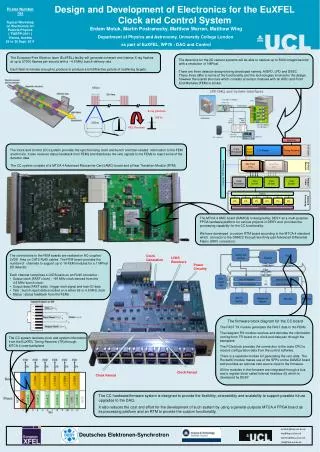
Test card A progress • The manufactured boards (PC3461M) are received • 8 boards in total • Initial test (voltages, LEDS) carried out – all working order • Each board provide 1 channel TX and 1 channel RX • 1 channel -> FAST clock, FAST data, Status, Veto -> 1 RJ45 conn. • AC coupling circuitries on the RX channel (clock,data,veto) • Further tests are carried out • A pair of boards used for telegram RX/TX and FAST RX/TX tests • 1st board -> Telegram TX – FAST RX • 2nd board -> Telegram RX – FAST TX • Tests were running successfully – without errors
Test card A progress • Stress testing the boards to verify the AC coupling circuitry • Random data pattern (LFSR generated) sent in between long durations of zeros or ones • Clock (99 MHz) is sent along with the data on a separate channel • Tests were run overnight using shielded cables (~5m) • No errors observed due to the AC coupling and the transmission • Results observed by ChipScope • A few errors observed due to the test firmware • The choice of the sync word is the cause – one random sequence is lost • Tests carried out on all 8 boards • Boards available to FEE developers if needed
UTCA crate progress • The purchased uTCA crate (xTCA) is kitted with the TR and the DAMC2 boards • SUSE Linux is installed on the crate • The boards were powered without any problems • IPMI tools detected the boards presence and the board information can be read • A simple test firmware to test the PCIe functionality of the DAMC2 board generated • DAMC2 board showed up on the PCIe tree without any problems • A simple test driver is generated for the board • Was able to access memory mapped registers on the board
RTM card progress • Schematic design for the RTM prototype is finished • The board provides 16 channels • 1 channel -> FAST clock, FAST data, Veto, Status Feedback • 1 spare channel (RJ45 connector) could also be fit • 2 pairs input (with the AC-coupling circuitry) • 2 pairs output (with the LVDS buffer) • Designed to provide maximum flexibility for testing • On-board (~9 MHz) oscillator • Clock multiplexers to select between on board clock and DAMC2 supplied clock • User programmable LEDs (on the 2x8 RJ45 connector) • Clock feedback to the DAMC2 board • Extra prototyping area
RTM card progress • RTM card designed according to the uTCA specs • Mechanical details to fit double width, full height faceplate • An I2C extender (PCF8574) • A temperature monitor () • An EEPROM () • Currently in the layout stage • Liaising with the RAL DO
Firmware progress • Joined the DESY-wide effort for standardising FPGA development for DAMC2 – FPGA Experts Group • A unified firmware/software framework to use the DAMC2 • A central project/core repository • Will use cores from the repository and contribute to it if needed • First aim is to provide a startup project for the DAMC2 • A general UCF file • PCIe block that is common to all cards • II Interface – A versatile bus/register interface between different cores on the FPGA • Cores for using SFP links, DDR2 RAM on board • Cores for using different peripherals – e.g. Clock MUX
Firmware progress • What this means for the CC card • The standard PCIe core for the DAMC2 is used • Based on Xilinx’s PCIe endpoint block + programmable memory access core • Standard Vendor ID + device ID for the DAMC2 card • Basic driver already been developed • A GUI to access individual registers (defined according to application) • II Bus/Interface will be used to integrate PCIe to CC related modules in the system • Individual registers + memory area defined in a VHDL package file • Use of internal and external registers and methods to access them
Firmware progress • Firmware block diagram with the II Interface • Control and clocking part involves cores for the clock MUX, synthesiser etc. on DAMC2 • The registers block on the old firmware diagram is replaced by II
Firmware progress • Telegram data transfer • Being redeveloped according to the latest • Basic serial transmit and receive module based on a UART like handshaking and synchronising is in the repository for the TR firmware • The telegram clock changed to 130 MHz • A protocol on top of this physical layer has to be defined for getting CC related information from the TR board • On-going work with P. Gessler and H. Kay • FAST data transmit • The existing module will be modified to integrate to the II interface
Veto logic • Use of the TPS (Toroid Protection System) for a possible VETO source • Developed by M. Werner and D. Noelle • A distributed system consisting of coils detecting the charge along the beam line plus their backend electronics • The analogue charge data is digitised and processed to provide information for MPS and other systems • A chain-like topology using digital fibre transmission lines to see how much charge has reached the next charge monitors Toroids Guns Undulator Undulator Linac Sections
Veto logic • Each toroid backend consists of a DAMC2 board and a custom RTM • SFPs on the DAMC2 are used for fibre communication to other toroids and other systems • Single-mode fibre – exact bit rate / protocol to be defined • One TX channel is available for the VETO system • Data from minimum two toroids envisaged for the VETO system • At the beginning and end of the undulators • Exact data to be determined (normalised charge data + train/bunch ID?) TX only @ 1.083 Gb/s (2.16 Gb/s ?) DAMC2 TPS SFPs (4 in total) TPS To FEEs VETO LOGIC on FPGA VETO FANOUT (RTM) Charge data from the TPS + Bunch ID ?
Future plans • RTM manufacture • Reception of the RTMs and initial testing • Card power-up important • Firmware debug/development • II Bus integration • Drivers • Testing the RTM + DAMC2 in the crates • Testing Standalone Operation • Testing with the TR (telegram/trigger/…) • Testing with the Test Card A (FAST data + clock) • VETO logic • TPS feasibility document • Initial work on VETO logic • Work on TPS data RX/TX ?