Download
1 / 2
20 likes | 115 Vues
Nanoscale Spin Transfer Devices and Materials Andrew D. Kent, New York University, DMR-0405620. I.

E N D
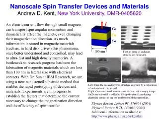
Nanoscale Spin Transfer Devices and MaterialsAndrew D. Kent, New York University, DMR-0405620 I An electric current flow through small magnets can transport spin angular momentum and dramatically affect the magnets, even changing their magnetization direction. As much information is stored in magnetic materials (such as, in hard disk drives) this phenomena, once better understood and controlled, may lead to ultra-fast and high density memories. A bottleneck to research progress has been the fabrication of magnetic materials which are less than 100 nm in lateral size with electrical contacts. With Dr. Sun at IBM Research, we are using a new nanostencil substrate method that enables the rapid prototyping of devices and materials. Experiments are in progress to establish the factors that determine the current necessary to change the magnetization direction and the efficiency of spin-transfer. Co Cu Co 100 nm First an array of undercut stencils are fabricated. Left: Then the desired layered structure is grown by evaporation of material onto the stencil. Right: Cross-sectional transmission electron microscopy image. Sufficient material is added to fill-up the stencil producing electrical contact to the top and bottom of the nanopillar. Physics Review Letters 93, 176604 (2004) Physical Review B 71, 140403 (2005) Additional information available at: http://www.physics.nyu.edu/kentlab/
Nanoscale Spin Transfer Devices and MaterialsAndrew D. Kent, New York University, DMR-0405620 • Education Post-doc:Jean-Marc Beaujour Graduate Students:Wenyu Chen, Barbaros Ozyilmaz (post-doc ,Columbia, 2005). Undergraduates: Mariano Zimmler (graduate student, Harvard, Fall 2004), Stuart Kirschner (graduate student, Johns Hopkins, Fall 2005), Brian Hayes, Lorraine Robinson, Alexandra Fries, James Lee and James Pyun High School Student: Yuriy Kagan, Intel Science Research (Columbia, Fall 2004) • Societal Impact Research of fundamental importance and critical to future magnetic information storage technology. Kent group at NYU involved in spin-transfer studies. Pictured above (left-right): Wenyu Chen, Andrew Kent, Barbaros Ozyilmaz, Jan Larsen, Jean-Marc Beaujour and Mariano Zimmler