Download
1 / 4
40 likes | 42 Vues
We are developing & producing Gallium Arsenide Wafers (GaAs wafers) & crystal using advanced crystal growth technology, such as VGF and GaAs wafer processing technology. Our quality GaAs wafers of 2~6 inch wafers are used in LED, lD and other Microelectronics applications industries.<br>http://www.qualitymaterial.net/products_2.html

E N D
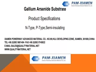
Gallium Arsenide Substrate Product Specifications N-Type, P-Type,Semi-insulating XIAMEN POWERWAY ADVANCED MATERIAL CO.- NO.99,HULI DEVELOPING ZONE, XIAMEN, 361000,CHINA TEL:+86 (0)592 5601404 -FAX:+86 (0)592 5745822 E-MAIL:SALES@QUALITYMATERIAL.NET WWW.QUALITYMATERIAL.NET
GaAs Wafers for LED Applications Item Specifications Remarks Conduction Type Growth Method Dopant Wafer Diamter Crystal Orientation OF Carrier Concentration Resistivity at RT Mobility Etch Pit Density Laser Marking Surface Finish Thickness Epitaxy Ready Package SC/n-type VGF Silicon 2, 3 & 4 inch (100)20/60/150 off (110) EJ or US (0.4~2.5)E18/cm3 (1.5~9)E-3 Ohm.cm 1500~3000cm2/V.sec <5000/cm2 upon request P/E or P/P 220~450um Yes Single wafer container or cassette SC/p-type with Zn dope Available Zn available Ingot or as-cut availalbe Other misorientation available
GaAs Wafers for LD Applications Item Specifications Remarks Conduction Type Growth Method Dopant Wafer Diamter Crystal Orientation OF Carrier Concentration Resistivity at RT Mobility Etch Pit Density Laser Marking Surface Finish Thickness Epitaxy Ready Package SC/n-type VGF Silicon 2, 3 & 4 inch (100)20/60/150 off (110) EJ or US (0.4~2.5)E18/cm3 (1.5~9)E-3 Ohm.cm 1500~3000 cm2/V.sec <500/cm2 upon request P/E or P/P 220~350um Yes Single wafer container or cassette Ingot or as-cut available Other misorientation available
GaAs Wafers,Semi-insulating for Microelectronics Applications Item Specifications Remarks Conduction Type Growth Method Dopant Wafer Diamter Crystal Orientation OF Carrier Concentration Resistivity at RT Mobility Etch Pit Density Laser Marking Surface Finish Thickness Epitaxy Ready Package Insulating VGF Undoped 2, 3, 4 & 6 inch (100)+/- 0.50 EJ, US or notch n/a >1E7 Ohm.cm >5000 cm2/V.sec <8000 /cm2 upon request P/P 350~675um Yes Single wafer container or cassette Ingot available