Download
1 / 23
400 likes | 925 Vues
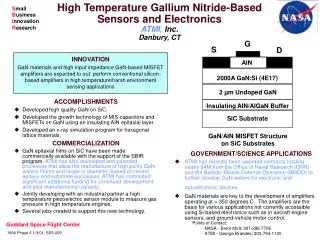
Gallium Nitride. Research & Development. Presented by Rakesh Sohal Supervision Prof. Dieter Schmeißer. GaN - Research & Development. Outline. Introduction GaN - Physics Crystal Growth MOVPE MBE Substrates & Buffer layers Recent Advances Applications.

E N D
Gallium Nitride Research & Development Presented by Rakesh Sohal Supervision Prof. Dieter Schmeißer
GaN - Research & Development Outline • Introduction • GaN - Physics • Crystal Growth • MOVPE • MBE • Substrates & Buffer layers • Recent Advances • Applications
GaN - Research & Development Why GaN ? • Semiconductor with Direct and Wide Bandgap • Optoelectronics Devices • Blue & Blue/green light emitters • Transistors withstand extreme heat and • High frequencies and power levels • More efficient amplifiers at base stations • Si-only 10% power used and 90% wasted as heat
a GaN - Research & Development GaN Physics Crystal Structure Zince Blende Wurtzite
GaN - Research & Development GaN Physics Energy band Structure
GaN - Research & Development GaN comparison Silicon cannot provide the power-bandwidth product for military applications
GaN - Research & Development GaN-Crystal Growth MOVPE Approach • First epilayer by vapour transport - Murusk and Tietjen (1969) • Growth rate - 0.5µm/min. • High background n-type carrier concentrations ~1019 cm-3 • Modern Technique - MOVPE by Nakamura • Key aspect : downward subflow of He and N2 • Claim - Improves the interaction of the reactant gases with the substrate • Shortcomings • High Substrate temperature • Thermal mismatch strain & defects
GaN - Research & Development GaN-Crystal Growth MBE Approach N - supplied by µ-wave plasma excitation provided by compact ECR Limited N-flux lower growth rate(GR) ~ 500Å/hr. GR can be increased by higher power Degraded Material Quality
GaN - Research & Development GaN-Crystal Growth Substrates for Epigrowth Baule Growth efforts are ongoing Till date - not possible The only Option - Heteroepitaxy The most Stringent Issue/Barrier
Hexagonal Cubic 3C-SiC ZnO MgO 6H-SiC 6.5 BN 650nm AlN Sapphire 5.5 AlN 4.5 650nm BN Band gap / eV 3.5 GaN GaN 650nm 2.5 650nm InN 650nm 1.5 4 2 2.5 3 3.5 4.5 5 5.5 Lattice Constant / Å GaN - Research & Development GaN-Crystal Growth Substrates for Epigrowth Thermal & lattice mismatch - Strain and Defects
GaN - Research & Development GaN-Crystal Growth Substrates for Epigrowth Thermal & lattice mismatch - Strain and Defects
Large lattice and thermal mismatch Strained and sometime cracked layers AlN GaN - Akashaki - Nakamura GaN - Research & Development GaN-Crystal Growth Interfacial buffer layer
GaN - Research & Development GaN-Advances Three major hurdles has been cleared • Heteroepitaxy - via buffer layer • Control of n (Si) & p(Mg)-type doping • Reduction in dislocation density Residual e-concentrations - --- due to N-vacancies(earlier) Van de Walle showed - energy required for Nv too high --- due to O incorporation
GaN - Research & Development GaN-Advances Use for patterned SiO2 Robert F. Davis, Proceedings of the IEEE, Vol. 90, No. 6, 2002
GaN - Research & Development Comparison - bulbs & LEDs
GaN - Research & Development New two flow MOCVD Nakamura‘s Method
GaN - Research & Development Pioneer of Nakamura • 1989-Started III-V nitride research. • 1990-Develops new ‘two-flow’ MOCVD equipment for growth of high quality single crystal GaN layers. • 1992-begins to grow InGaN single crystal layers for the production of double heterostructures. • 1993-Succeeded in developing a blue LED with a luminous intensity as high as 2cd using III-V nitride materials. • 1995-Developed high-brightness SQW structure blue/green LEDs with a luminous intensity of 2 cd and 10 cd, and developed a violet laser diode using III-V nitride materials for the first time. • 1996-The first current infection III-V nitride based LDs were fabricated. • 1996-Announces the first CW blue GaN based injection laser at room temperature.
GaN - Research & Development Steps to grow crystalline GaN Nakamura‘s Method The substrate was heated to 1050oC in a stream of hydrogen The thickness of the GaN buffer layer was varied between 100Å and 1200Å The substrate temperature was lowered to between 450oC and 600oC to grow the GaN buffer layer. The total thickness of the GaN film was about 4 mm,and the growth time was 60 min. The substrate temperature was elevated to between 1000oC and 1030oC to grow the GaN film.
GaN - Research & Development Buffer layer thickness The value of the FWHM is almost constant between 200Å and 1200Å thickness.The optimum thickness of the GaN buffer layer was around 200Å
GaN - Research & Development GAN - Potential
GaN - Research & Development Applications • Large scale displays (large outdoor television screens) • Smaller full-color flat panel display screens (inside trains or subway stations) • Full-color scanners • Full-color photocopying machines • Full-color FAX machines • Traffic lights • LED white lamps
GaN - Research & Development Applications 2 inch dia blue LED wafer on GaN-on-sapphire
GaN - Research & Development Thanks for your attention!