Download
1 / 1
30 likes | 214 Vues
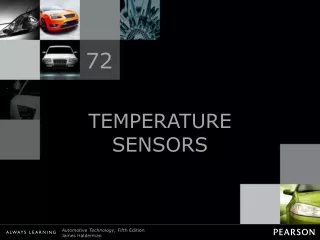
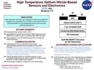
G. S. D. AIN. 2000A GaN:Si (4E17). 2 µm Undoped GaN. Insulating AIN/AIGaN Buffer. SiC Substrate. S mall B usiness I nnovation R esearch. High Temperature Gallium Nitride-Based Sensors and Electronics ATMI, Inc. Danbury, CT. INNOVATION.

E N D
G S D AIN 2000A GaN:Si (4E17) 2 µm Undoped GaN Insulating AIN/AIGaN Buffer SiC Substrate Small Business Innovation Research High Temperature Gallium Nitride-BasedSensors and ElectronicsATMI, Inc.Danbury, CT • INNOVATION GaN materials and high input impedance GaN-based MISFET amplifiers are expected to out perform conventional silicon-based amplifiers in high temperature/harsh environment sensing applications ACCOMPLISHMENTS • Developed high quality GaN on SiC. • Developed the growth technology of MIS capacitors and MISFETs on GaN using an insulating AIN epitaxial layer. • Developed an x-ray simulation program for hexagonal lattice materials. COMMERCIALIZATION • GaN epitaxial films on SiC have been made commercially available with the support of the SBIR program. ATMI has also developed and patented processes that allow the manufacture of high purity GaN wafers 50mm and larger in diameter. Based on recent epitaxy and substrate successes, ATMI has committed significant additional funding for continued development and pilot manufacturing capacity. • Jointly developing with an industrial partner a high temperature piezoelectric sensor module to measure gas pressure in high temperature engines. • Several jobs created to support this new technology. GaN/AIN MISFET Structure on SiC Substrates • GOVERNMENT/SCIENCE APPLICATIONS • ATMI has recently been awarded contracts totaling nearly $4M from the Office of Naval Research (ONR) and the Ballistic Missile Defense Operation (BMDO) to further develop GaN wafers for electronic and optoelectronic devices. • GaN materials are key to the development of amplifiers operating at > 350 degrees C. The amplifiers are the basis for various applications not currently accessible using Si-based electronics such as in aircraft engine sensors, and ground-vehicle motor control. Points of Contact: - NASA - Brent Mott; 301-286-7708 - ATMI - George Brandes; 203-794-1100 Goddard Space Flight Center 1994 Phase II 1/3/01; SS5-009