Download
1 / 4
40 likes | 51 Vues
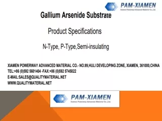
We are developing & producing Gallium Arsenide Wafers (GaAs wafers) & crystal using advanced crystal growth technology, such as VGF and GaAs wafer processing technology. Our quality GaAs wafers of 2~6 inch wafers are used in LED, lD and other Microelectronics applications industries.<br>http://www.qualitymaterial.net/products_2.html

E N D
PAM-XIAMEN specializes in GaN-based ultra high brightness blue and green light emitting diodes (LED) and laser diodes (LD). Also we offer GaN Free-standing wafer and GaN Templates(GaN-on-Sapphire). GaN Wafer Product Specifications XIAMEN POWERWAY ADVANCED MATERIAL CO.- NO.99,HULI DEVELOPING ZONE, XIAMEN, 361000,CHINA TEL:+86 (0)592 5601404 -FAX:+86 (0)592 5745822 E-MAIL:SALES@QUALITYMATERIAL.NET WWW.QUALITYMATERIAL.NET
GaN on Al2O3-2” epi wafer Specification White: Blue: Green: : 445~ : 465~ :510~ ~460 nm ~475 nm ~530 nm 1. Growth Technique - MOCVD 2.Diameter: 50.8mm 3.Substrate material: Patterned Sapphire Substrate(Al2O3) 4.Pattern size: 3X2X1.5µm 5.Structure: Structure layers Thickness(µm) p-GaN p-AlGaN InGaN/GaN(active area) 0.2 0.03 0.2 2.5 2 430 n-GaN u- GaN Al2O3 (Substrate) 6.Parameters to make chips: Item Color Chip Size Characteristics Appearance Application Lighting LCD backlight Mobile appliances Consumer electronic Vf = 2.8~3.4V Po = 18~25mW Wd = 450~460nm PAM1023A01Blue 10mil x 23mil Vf = 2.8~3.4V Po = 250~300mW Wd = 450~460nm General lighting LCD backlight Outdoor display PAM454501 Blue 45mil x 45mil *If you need to know more detail information of Blue LED Chip, please contact with our sales departments
2" GaN Template Item PAM-GaNT-N PAM-GaNT-SI Conduction Type Size Thickness Orientation Resistivity(300K) Dislocation Density Substrate Structure Surface Finish Usable Area N-type Semi-insulating 2"(50mm) dia. 20um,30um 30um,90um C-axis(0001)+/-1O <0.05Ω·cm >1x10⁶Ω·cm <1x108cm-2 Thick GaN on Sapphire(0001) Double Side Polished,epi-ready ≥ 90 % 2"GaN Free-standing Wafer Item PAM-GaN50-N PAM-GaN50-SI Conduction Type Size Thickness Orientation Resistivity(300K) Dislocation Density Marco Defect Density Surface Finish Usable Area N-type Semi-insulating 2"(50mm) dia. 230+/-20um, 280+/-20um C-axis(0001)+/-1O <0.05Ω·cm >1x10⁶Ω·cm <5x106cm-2 <5cm-2 Double Side Polished,RMS<2nm,N-Face RMS<1µm,epi-ready ≥ 90 %
10mm*10.5mm,GaN Free-standing Wafer Item PAM-GaN50-N PAM-GaN50-SI Conduction Type Size Thickness Orientation Resistivity(300K) N-type Semi-insulating 10mmx10.5mm 230+/-20um, 280+/-20um C-axis(0001)+/-1O <0.05Ω·cm >1x10⁶Ω·cm Dislocation Density Marco Defect Density Surface Finish <5x106cm-2 <5cm-2 or 5-10cm-2 Double Side Polished,RMS<2nm,N-Face RMS<1µm,epi-ready <5cm-2 ≥ 90 % Usable Area