
Uploaded by
raanan
1 SLIDES
715 VUES
140LIKES
Electron Beam
DESCRIPTION
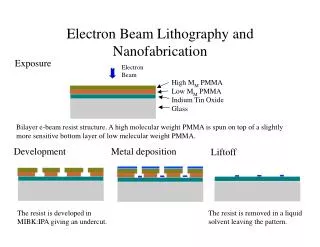
Electron Beam Lithography and Nanofabrication. Exposure. Electron Beam. High M M PMMA Low M M PMMA Indium Tin Oxide Glass. Bilayer e-beam resist structure. A high molecular weight PMMA is spun on top of a slightly more sensitive bottom layer of low melecular weight PMMA. Development.
Download
1 / 1
Télécharger la présentation 
Electron Beam
An Image/Link below is provided (as is) to download presentation
Download Policy: Content on the Website is provided to you AS IS for your information and personal use and may not be sold / licensed / shared on other websites without getting consent from its author.
Content is provided to you AS IS for your information and personal use only.
Download presentation by click this link.
While downloading, if for some reason you are not able to download a presentation, the publisher may have deleted the file from their server.
During download, if you can't get a presentation, the file might be deleted by the publisher.
E N D
Presentation Transcript
Electron Beam Lithography and Nanofabrication Exposure Electron Beam High MM PMMA Low MM PMMA Indium Tin Oxide Glass Bilayer e-beam resist structure. A high molecular weight PMMA is spun on top of a slightly more sensitive bottom layer of low melecular weight PMMA. Development Metal deposition Liftoff The resist is developed in MIBK:IPA giving an undercut. The resist is removed in a liquid solvent leaving the pattern.


More Related