Electron Beam Lithography. William Whelan-Curtin. What is EBL for?. LPN. Nanopatterning High Precision Reliable Versatile . What is needed?. Very narrow, precisely controllable beam of Electrons Lots of money, a big complex machine, and a lot of expertise! . Outline.
Une image / un lien ci-dessous est fourni (tel quel) pour télécharger la présentation
Politique de téléchargement : le contenu du site vous est fourni TEL QUEL pour votre information et votre usage personnel ; il ne peut être vendu, concédé sous licence ni partagé sur d’autres sites sans l’accord de son auteur.Le contenu vous est fourni TEL QUEL, pour votre information et votre usage personnel uniquement.Téléchargez la présentation en cliquant sur ce lien.Lors du téléchargement, si vous ne parvenez pas à télécharger une présentation, l’éditeur a peut-être supprimé le fichier de son serveur.Pendant le téléchargement, si vous ne parvenez pas à obtenir une présentation, le fichier a peut-être été supprimé par l’éditeur.
Types of Electron Beam Writer • SEM (Electron Beam “Reader”) • Generally magnetic lenses • Up to 30kV • Converted SEM (RAITH) • Addition of (fast) beam blanker • Pattern generator • Deflection needs time to stablise raster scan vector scan
Types of Electron Beam Writer • Purpose Built (LEICA/JEOL) • Better control, calibration • Up to 100kV • Higher speeds • Bigger writefields • Secondary deflection system Can also correct for aberrations in the primary lens
Types of Electron Beam Writer • Shaped Beam systems • Very complex optics • Higher current, lower resolution • Photomask making • (Not a research tool) GAUSSIAN
Patterning LPN • Electron sensitive polymer- the “paper”
Electron-Solid Interactions Primary electrons • Secondary electrons • Low energy (50eV) • Low penetrating power Responsible for exposure
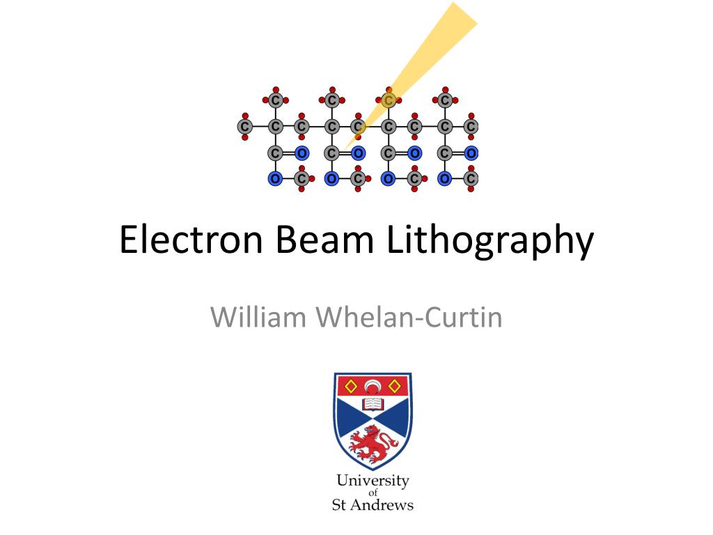
H H H H C C C C H H H H H H H H H H H H H H C C C C C C C C C C C H H H H H O C O C O C C O n H H H H C O C O C O C O H H H H H H H H Electron Sensitive resist • Poly methyl methyl acrylate • Spin Coating • Long polymer chains H H C C H H H H H H C C C H H C C O O H H O O C C H H H H PMMA Substrate
H H C C C C H Electron Sensitive resist Secondary Electrons • Bonds broken (induced chain scission) • Dissolved by suitable chemical • Methyl Isobutyl ketone • Isopropanol:Water H H H H H H C C C C C C H H H H H H H H H H H H H H H H H H C C C C C C C C C C H H H H H H C C O O O C O C O C C O n H H H H H H O O C C C O C O C O C O H H H H H H H H H H H H PMMA Substrate
Contrast Curve Function of: Voltage Resist Thickness Substrate e.g. 170uAs/cm2 for 500nm thick PMMA on Silicon @ 30kV • Threshold electron density (lower≡faster exposure) • “Clearing Dose” or “Base Dose” • Slope -> Resolution Resist Thickness Dose (electrons/area)
Contrast Curve- Experimental • Determine for each new situation • Recheck regularly • Problem diagnosis Dose 50um
H H C C C C H Negative Resist Secondary Electrons • Microchem SU8 • Photo acid generator • Baking • Crosslinking • Acid Diffusion H H H H H H C C C C C C H H H H H H H H H H H H H H H H H C C C C C C C C C C H H H H H H C C O O O C O C O C C O n H H H H H H O O C C C O C O C O C O H H H H H H H H H H H H SU8 Substrate
Contrast Curve • Threshold electron density • Chemical amplification • Lower clearing dose Resist Thickness e.g. 1uAs/cm2 for 200nm thick SU8 on Silicon @ 30kV Dose (electrons/area)
Resolution J. Vac. Sci. Technol. B 12, 1305 (1975) • Most EBL systems -> 1nm spot sizes or less Vb 1nm Rt df df = effective beam diameter (nm) Rt = resist thickness (nm) Vb = acceleration voltage (kV)
Resolution EBL advice: Keep resist as thin as possible
EBL vs Focused Ion Beam etching • FIB • Energetic Gallium ions • Etching of the material • EBL • Modification • No removal of material Heavy ions Substrate
Electron-Solid Interactions Unintended Exposure! Primary electrons • Secondary electrons • Low energy (50eV) • Low penetrating power
Parameters • Depend on voltage/resist/substrate • Determine in each instance • Monte Carlo simulations • Experiment L. Stevens et al., Microelectronic Engineering 5, 141-150 (1986)
Correction Programs • Nanopecs, Proxecco • Pattern • Fracture • Calculate electron distributions • Alter pattern • Recalculate • Iterate until convergence is reached
Laser Stage • Limited Deflection • Expose one “writefield” at a time • Laser interferometer controlled Stage movements • Calibrated • Sub 40nm accuracy • Pattern stitched together • Critical for Photonics