1 / 29

Electron Beam Lithography at the Center for Nanotechnology

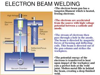
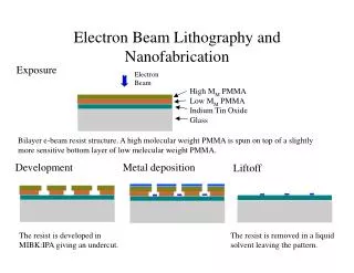
Electron Beam Lithography. Pattern Writing system capable of producing fine linewidths ~ 20nm.Scanning raster of E beam over resist coated substrate.First developed in 1960s using existing SEM technology.. . Standard Lithography Uses. Maskmaking

gaius
Télécharger la présentation

Electron Beam Lithography at the Center for Nanotechnology

An Image/Link below is provided (as is) to download presentation Download Policy: Content on the Website is provided to you AS IS for your information and personal use and may not be sold / licensed / shared on other websites without getting consent from its author. Content is provided to you AS IS for your information and personal use only. Download presentation by click this link. While downloading, if for some reason you are not able to download a presentation, the publisher may have deleted the file from their server. During download, if you can't get a presentation, the file might be deleted by the publisher.

E N D

Presentation Transcript


    1. Electron Beam Lithography at the Center for Nanotechnology Greg Golden

More Related