e-Beam Lithography
e-Beam Lithography. Antony D. Han Chem 750 U of Waterloo 06-02-07. What is lithography?. Original meaning: a process of printing using a non-polar ink applied to a hydrophilic master plate patterned with a hydrophobic image. Modern usage

e-Beam Lithography
E N D
Presentation Transcript
e-Beam Lithography Antony D. Han Chem 750 U of Waterloo 06-02-07
What is lithography? • Original meaning: • a process of printing using a non-polar ink applied to a hydrophilic master plate patterned with a hydrophobic image. • Modern usage • The term is more generally applied to a number of methods for replicating a predetermined master pattern on a substrate. • Replication is effected by first coating the substrate with a radiation-sensitive polymer film (a resist) and then exposing the film to actinic radiation in a pattern-wise manner. The radiation chemistry that results alters the physical or chemical properties of the exposed areas of the film such that they can be differentiated in a subsequent image development step. Most commonly, the solubility of the film is modified with the radiation chemistry either increasing the solubility of exposed areas (yielding a positive image of the mask after develop) or decreasing the solubility to yield a negative-tone image of the mask. • Widely used in semiconductor industry and IT industry. • Focused eBL: ~sub 50 nm resolution
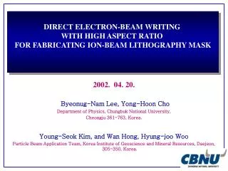
Steps involved in the EBL process. With a beam current of 600 pA and an accelerating voltage of 100 kV, the beam diameter was approximately 3 nm. J. Phys. Chem. B 2002, 106, 11463-11468
e-Beam Lithography • Electron source: SEM • Equipment: SEM equipped with a pattern generator and alignment system • e-beam control: • accelerating voltage (kV) • operation current (pA) • exposure dose (µC/cm2) • exposure dwell period (µs)
eBL followed by SA Langmuir, Vol. 20, No. 9, 2004, 3495
eBL changes the properties of coating layers Langmuir, Vol. 20, No. 9, 2004 3767
Applications of eBL (a) Backscattered electron (BSE) image of ZnO patterns on SiOxsubstrates annealed in air at 700 °C for 20 min (b) secondary electron (SE) image before annealing (c) SE image after annealing at 700 °C for 20 min in air (d) SE image of annealed patterns over a large area. Nano Lett., Vol. 5, No. 9, 2005
Applications of eBL Proceedings of SPIE Vol. 5184
Limitation • Tradeoffs for high-resolution • Time and high resolution • Improvement wrt this limitation • More sensitive resists • Cold developers (<10 ºC)
eBL applications Langmuir, Vol. 20, No. 9, 2004 3767