E-beam Evaporation
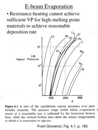
E-beam Evaporation. Resistance-heating cannot achieve sufficient VP for high-melting point materials to achieve reasonable deposition rate. From Grovenor, Fig. 4.1, p. 180. E-beam Evaporation. Use an electron beam to provide the necessary heating.

E-beam Evaporation
E N D
Presentation Transcript
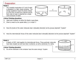
E-beam Evaporation • Resistance-heating cannot achieve sufficient VP for high-melting point materials to achieve reasonable deposition rate From Grovenor, Fig. 4.1, p. 180
E-beam Evaporation • Use an electron beam to provide the necessary heating • A hot filament emits electrons by thermionic emission • The electrons are accelerated to the source through a potential difference of several to 15 kV • The electrons are steered by a B-field via the Lorentz force to strike the material to be evaporated from Mahan, Fig. V.2(a), p. 116
E-beam Evaporation from Mahan, Fig. I.3, p. 3
E-beam Evaporation from Ohring, Fig. 3-12, p. 100
E-beam Evaporation from Ohring, Table 3-3, p. 102
E-beam Evaporation from Ohring, Table 3-3, p. 103
E-beam Evaporation • Advantages : • Electron K.E. is transferred as heat to the evaporant causing it to locally melt; this avoids contamination from the container • Hot crucibles are not in the line of sight of the substrate • Disadvantage : • Energetic electrons and x-ray radiation may damage some films so sputtering or CVD has replaced e-beams for some applications (e.g., MOS devices)