Download
1 / 25
250 likes | 356 Vues
Explore innovative sensor designs based on periodically segmented waveguides and active lasing technology using critical sensitivity effects. Collaborate with experts from Tel-Aviv University to develop advanced optical sensors for various projects. Utilize porous silicon material for enhanced surface interaction area, simplicity in fabrication, and compatibility with technology. Implement multi-sensing principles for gas detection and biochemical analysis. Experiment with DNA hybridization, toxic detection, and antigen binding. Enhance dynamic range and eliminate phase ambiguity in wavelength-interrogated interferometric sensors.

E N D
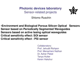
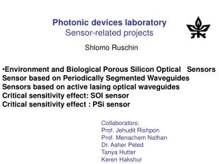
Photonic devices laboratorySensor-related projects • Environment and Biological Porous Silicon Optical SensorsSensor based on Periodically Segmented WaveguidesSensors based on active lasing optical waveguidesCritical sensitivity effect: SOI sensorCritical sensitivity effect : PSi sensor Shlomo Ruschin Collaborators:Prof. Jehudit RishponProf. Menachem NathanDr. Asher PeledTanya HutterKeren Hakshur
Tel-Aviv University Porous Silicon Optical Sensors Tanya Hutter and Shlomo Ruschin
Ammonia storage warehouse ALARM ! NH3 NH3 NH3 NH3 NH3 NH3 Motivation (1) porous silicon sensors Light source and receiving fiber PSi Sensors ADVANTAGES: • Cheap • Small • Remote • Passive (can be used in flammable environment)
Motivation (2) porous silicon sensors • Breath analysis for clinical applications Ammonia is listed as one of the marker molecules that can identify kidney impairment.
500 nm Porous silicon • Porous silicon (PSi) is a material formed by electrochemical etching of crystalline silicon. • ‘nano-sponge’
Porous silicon (PSi) - Why !?!? • Increased surface interaction area 200-1000 m2/cm3. • Simplicity and repeatability of fabrication. • Ability to produce pores in the range of 30Å to 1μm and porosities of 10-90%. • Compatibility with technology: easily integrable with Si-based microelectronics. • Biocompatible H. Ouyang et al., Frontiers in Surface Nanophotonics, 2007
Outlet Gas chamber White light source Porous Silicon Spectrometer Humidifier Flowmeters NH3 Gas N2 Gas Optical Measurement Setup • Light from tungsten-halogen lamp passes through collimating lens. • The reflected rays are collected and transmitted to a PC via spectrometer. • The reflected spectra is collected at wavelengths 400-1000nm. Experimental optical setup
Ammonia vapor & pH indicator • After Exposure: ammonia reacts with BTB, and the sample changes its color from yellow to blue. The reflected spectrum Yellow absorbance at 400-430nm Blue absorbance at 550-650nm
Multi-Sensing Principle Gas out Porous silicon surface Gas in
Multi-Sensing Principle • Sensor array concept. • Each section is made of porous silicon with a different functionality. • White light is collimated to illuminate the entire sample. • The reflected light from all the sections is measured simultaneously in a non-imaging configuration using a single detector. • The obtained spectrum consists of many overlapping interference spectra each reflected from a different sensor section.
Model system: Biotin-Avidin PSi sample before and after biotin connection to the PSi sensor. PSi sample before and after Avidin connection to the PSi sensor.
Periodically Segmented Waveguides and sensors based upon them
The basic PSW-MZI sensor Processing is simpler (single photolithography step)
Examples of sensing systems experimentally tested: • DNA Hybridization • Toxics- Parathion hydrolase • Antigen binding (Biotin-Avidin)
Concept Sensor l Pump Architecture & detection scheme Suitable for both remote sensing & biomedical device
Monolithic rare-earth doped sol-gel tapered rib waveguide laser Nd-doped tapered rib waveguide laser- schematic view, not drawn to scale for clarity
Output lasing power as a function of input pump power for different pump wavelengths Emission spectra of the laser device for different input pump powers.
Critical sensitivity effect in an interferometer sensor Ronen Levy, Shlomo Ruschin*, and Damian Goldring 2mm
Critical sensitivity effect in an interferometer sensor Ronen Levy, Shlomo Ruschin*, and Damian Goldring Splitting effect Sensor output power for the scanned wavelength range without illumination (Blue, solid line) and with illumination (Green, dashed line).
Dynamic Range Enhancement and Phase-Ambiguity Elimination in Wavelength-Interrogated Interferometric Sensor Tanya Hutter,1 Stephen R. Elliott,1 and Shlomo Ruschin2,*