Microprocessor History
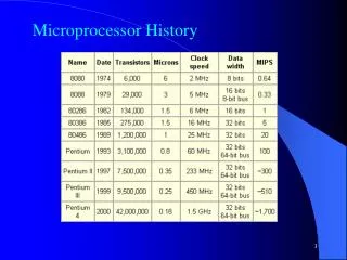
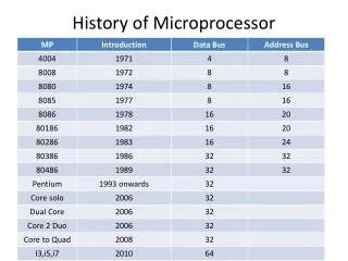
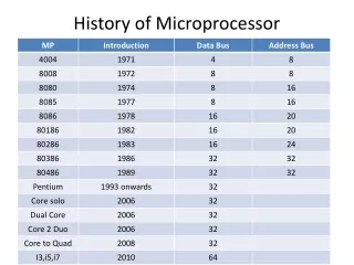
Microprocessor History. Early microprocessors. PMOS technology – slow and awkward to interface with TTL family 4 bit processor Instructions were executed in about 20 µs. Intel 4004 the first MP. 4K nibbles address space. Intel 8008- can manipulate a whole byte. 16Kbytes address space

Microprocessor History
E N D
Presentation Transcript
Microprocessor History created by :Gaurav Shrivastava contact:-gaurav9915969367@ymail.com
Early microprocessors • PMOS technology – slow and awkward to interface with TTL family • 4 bit processor • Instructions were executed in about 20 µs. • Intel 4004 the first MP. 4K nibbles address space. • Intel 8008- can manipulate a whole byte. • 16Kbytes address space • 50,000 operations/second. created by :Gaurav Shrivastava contact:-gaurav9915969367@ymail.com
N-channel MOSFET • 1970. • Faster than P-MOS. • Work with +ve supply; easy to interface with TTL. • 1973 Intel 8080 MP. • 500,000 operations/second. • 64K bytes memory. • Upward software compatible with 8008. • Other brands are MC6800, Fairchild’s F-8 etc. created by :Gaurav Shrivastava contact:-gaurav9915969367@ymail.com
Basic types of MP • Two types • Single component microprocessors • Bit sliced microprocessors • Can be cascaded to allow functioning systems with word size from 4 bits to 200 bits. created by :Gaurav Shrivastava contact:-gaurav9915969367@ymail.com
Single component M Computer • Composed of • A processor • read only memory (for program storage) • Read/Write memory (for data storage) • Input/output connections for interfacing • Timer as event counter • Intel 8048, Motorola 6805R2. • Oven, washing machine, dish washer etc. created by :Gaurav Shrivastava contact:-gaurav9915969367@ymail.com
Modern MP • 8, 16, 32, 64 bits are available. • Intel 8085, Motorola 6800 – 8 bit word 16 bit address. • Intel 8088, 8086, Motorola 68000 – 16 bits word, 20 bits address. • 80186 – never used. • 286 – real mode and protected mode; 16MB memory • 386 – paging, 4GB memory, 32 bits word • 486 – math coprocessor, L1 cache created by :Gaurav Shrivastava contact:-gaurav9915969367@ymail.com
Modern MP • Pentium • 64 bits i/o off the chip but process 32bits word, exception floating point processed 64 bits, cache doubled, instruction pipelining. • Pentium Pro • L2 cache, Improved pipelining • Pentium MMX • Multi-Media extensions, 57 new inter instruc mostly used for multimedia programming • Pentium II, III, IV • Pentium pro with MMX tech, increased L2 cache, full 64 bit operation • RISC • Reduced instruction set processor, uniform length instruc, faster in operation, cannot perform may different thing as CISC. created by :Gaurav Shrivastava contact:-gaurav9915969367@ymail.com
Basic MP architecture Data Bus • Fetch, decode, execute. • PC increment. • First instruction is a fetch • 0000H for 8085 • FFFF0H for 8086, 8088 AF, BC, DE, HL, SP, PC many more Register Array Instruction Register ALU Control Bus control Address Bus created by :Gaurav Shrivastava contact:-gaurav9915969367@ymail.com
Memory Interfacing and IO decoding created by :Gaurav Shrivastava contact:-gaurav9915969367@ymail.com
Interfacing needs bus • Isolation and separation of signals from different devices connected to MP. • Unidirectional • Bidirectional • LS373, 244 created by :Gaurav Shrivastava contact:-gaurav9915969367@ymail.com
Memory map • Pictorial representation of the whole range of memory address space. • Defines which memory system is where, their sizes etc. • Address space or range. • 8086 has 1M address space in minimum mode. • 8085 has 64K address sspace. created by :Gaurav Shrivastava contact:-gaurav9915969367@ymail.com
Address Decoding • Address decoder is a digital ckt that indicates that a particular area of memory is being addressed, or pointed to, by the MP. • Absolute address decoding • Decode an address to one single output • Decode 10110 so that u can get a signal from the decoder when it receives exactly that bit pattern. • Partial address decoding • Some bits are used as don’t care so that decoder gives a signal for a range of consecutive bit patterns. created by :Gaurav Shrivastava contact:-gaurav9915969367@ymail.com
Absolute decoding 1 0 1 1 0 1 0 1 1 0 a b c d e Active low o/p signal a b c d e Can use decoder IC with gates to achieve exact decoded o/p 0 3 to 8 line dcd 1 0 1 o/p Logic 1 7 8 input NAND gate implementation created by :Gaurav Shrivastava contact:-gaurav9915969367@ymail.com
Partial decoding • When a range of addresses are deconded then it is called partial decoding. For example, if we need to generate a control signal for an address generated by the MP within the range FFF0 – FFFF, then it is called partial decoding. • Decoder, multiplexer can be used for address decoding A15 A14 1 1 1 1 1 1 1 1 1 1 1 1 x x x x A4 created by :Gaurav Shrivastava contact:-gaurav9915969367@ymail.com
Internal architecture of 8085 ALU created by :Gaurav Shrivastava contact:-gaurav9915969367@ymail.com
Flag register • S : after the execution of an arithmetic operation, if bit 7 of the result is 1, then sign flag is set. • Z : bit is set if ALU operation results a zero in the Acc or registers. • AC: bit is set, when a carry is generated by bit 3 and passed on bit 4. • P: parity bit is set when the result has even number of 1s. • CY = carry is set when result generates a carry. Also a borrow flag. S Z AC P CY created by :Gaurav Shrivastava contact:-gaurav9915969367@ymail.com
Accumulator • Hold data for manipulation (arithmetic, logical). • Whenever the operation combines two words, either arithmetically or logically, the accumulator contains one word (say A) and the other word(say B) may be contained in a register or in memory location. After the operation the result is placed in the Acc replacing the word A. • Major working register. MP can directly work on Acc. • Programmed data tranfer. created by :Gaurav Shrivastava contact:-gaurav9915969367@ymail.com
General purpose registers • Six registers. • B, C, D, E, H and L can store 8 bit data. • They can be combined to perform some 16 bit operation. created by :Gaurav Shrivastava contact:-gaurav9915969367@ymail.com
ALU • Arithmetic logic unit. • Two input ports, one output port. • Perform AND, OR, ExOR, Add, subtract, complement, Increment, Decrement, shift left, shift right. • ALUs two temporary registers are connected to MPs internal bus from which it can take data from any registers. It can place data directly to data bus through its single output port. created by :Gaurav Shrivastava contact:-gaurav9915969367@ymail.com
Program counter • Its job is to keep track of what instruction is being used and what the next instruction will be. • For 8085 it is 16 bit long. • Can get data from internal bus as well as memory location. • PC automatically increments to point to the next memory during the execution of the present instruction. • PC value can be changed by some instructions. created by :Gaurav Shrivastava contact:-gaurav9915969367@ymail.com
Stack pointer • 16 bit register acts as memory pointer. • Can save the value of the program counter for later use. • points to a region of memory which is called stack. follows LIFO algorithm. • After every stack operation SP points to next available location of the stack. Usually decrements. created by :Gaurav Shrivastava contact:-gaurav9915969367@ymail.com
Memory address register • PC sends address to MAR. MAR points to the location of the memory where the content is to be fetched from. • PC increments but MAR does not. • If the content is an instruction, IR decodes it. During execution if it is required to fetch another word from memory, PC is loaded with the value • PC again sends it to the MAR and fetch operation starts. created by :Gaurav Shrivastava contact:-gaurav9915969367@ymail.com
Instruction register • Holds instruction the micro is currently being executed. • 8 bit long. created by :Gaurav Shrivastava contact:-gaurav9915969367@ymail.com
others • Instruction decoder. • Control logic. • Internal data bus. created by :Gaurav Shrivastava contact:-gaurav9915969367@ymail.com
8085 5V GND 40 20 21 – 28 HIGH ORDER ADD BUS X1 X2 SID 5 SOD 4 • 40 pin DIP. • +5V • 3 - 5MHz • ADD BUS • DATA BUS • CONTROL STATUS • POWER SUPPLY AND FREQ • EXTERNALLY INITIATED SIGNALS • SERIAL I/O PORTS TRAP 6 12 – 19 MUX ADD/ DATA BUS RST7.5 7 RST6.5 8 RST5.5 9 INTR 10 30 ALE 29 S0 READY 35 HOLD 39 33 S1 RESET IN 36 34 IO/M’ 32 RD’ INTA 11 31 WR’ HLDA 38 3 37 created by :Gaurav Shrivastava contact:-gaurav9915969367@ymail.com CLK OUT RESET OUT
A15 Address bus. higher 8 bit A8 ALE G Address bus. Lower 8 bit AD7 D Q’ AD6 AD5 Data bus AD0 GND OC ADD/DATA bus • Address bus 16 bits • A8 to A15 unidirectional. Higher 8 bit • AD0 to AD7 multiplexed with data. This pins are bidirectional when used as data bus. • Data bus 8 bit long: AD0 to AD7 created by :Gaurav Shrivastava contact:-gaurav9915969367@ymail.com
Control signals • ALE – active high output used to latch the lower 8 address bits. • RD, WR - active low output signals. • IO/M – output signal to differentiate memory and IO operation. • S1 and S0 – status output signal. Identify various operations. created by :Gaurav Shrivastava contact:-gaurav9915969367@ymail.com
External control signals • INTR – interrupt request. Input signal • INTA – interrupt acknowledge. o/p signal. • RST7.5,RST 6.5, RST5.5 – restart interrupts. Vectored interrupts. Higher priority. • TRAP - Nonmaskable interrupt. Highest priority. • Hold – request for the control of buses. O/P signal • HLDA – Hold Acknowledge. I/P signal • READY – I/P signal. When low Mp waits for integral number of clock cycles until it goes high. created by :Gaurav Shrivastava contact:-gaurav9915969367@ymail.com
MEMR 8085 IO/M IOWR RD MEMWR WR IOWR Bus control signals created by :Gaurav Shrivastava contact:-gaurav9915969367@ymail.com
MUX W Temp Reg (8) Z Temp Reg (8) B (8) C (8) D (8) E (8) Reg Select H (8) L (8) Stack pointer (16) Program counter (16) Incrementer/decrementer Latch (16) 8080 functional block diagram Serial I/O control Interrupt control Temp Reg Accumu Instru Register (8) Instru Decoder Flags Address buffer (8) Data/Add buffer (8) Timing & control created by :Gaurav Shrivastava contact:-gaurav9915969367@ymail.com
Timing diaga. of Memory cycle T1 T2 T3 T1 T2 T3 CLK A15-A8 Data from memory A7-A0 Data from MPU AD7-AD0 A7-A0 ALE IO/M RD WR MEMRD MEMWR WRITE Cycle READ Cycle created by :Gaurav Shrivastava contact:-gaurav9915969367@ymail.com
CE Interfacing A Memory Chip • 2K Byte memory • Memory address space of the chip: • 8800H to 8FFFH A14 A15 IO/M A13 E1 E2 E3 3 to 8 decoder A12 MEMSEL Q1 A11 Memory Chip A10 D7 A9 D6 A15 A14 A13 A12 A11 A10 A9 A8 A7 A6 A5 A4 A3 A2 A1 A0 1 0 0 0 1 X X X X X X X X X X X A0 D0 RD 8 8 - F 0 - F 0 - F WR created by :Gaurav Shrivastava contact:-gaurav9915969367@ymail.com
MVI A,32H Instruction M1 (Opcode-fetch) M2 (Memory Read) 2000H 3EH ;MVI A, 32H 2001H 32H T3 T1 T2 T3 T2 T4 T1 A15-A8 20H; high-order address Unspecified 20H; High-order address 01H; low-order Add 00H; low-order Add 32H; Data AD7-AD0 3E; opcode ALE Status IO/M=0,S1=1,S0=1; opcode fetch Status IO/M=0,S1=1,S0=0; data read RD created by :Gaurav Shrivastava contact:-gaurav9915969367@ymail.com
OUT/IN instruction • port address: 50H 2050 D3 2051 50 • Let input port address is 30H 2150 DB 2151 30 OUT 50H sends acc content to I/O address 50H IN 30H reads content from I/O address 30H and stores the value in accum created by :Gaurav Shrivastava contact:-gaurav9915969367@ymail.com
21H 51H Port addre 30H IN 30H instruction M1 M2 M3 T1 T2 T3 T4 T1 T2 T3 T1 T2 T3 CLK unspecified 21H Port add 30H A15-A8 Data from Accumula DB from memory 50H AD7-AD0 Port add 30H ALE IO/M RD MEMRD IORD created by :Gaurav Shrivastava contact:-gaurav9915969367@ymail.com
unspecified 20H 20H Port add, 50H Port addre 50H Opcode D3 Data from Accumula Port add 50H 50H 51H OUT 50H instruction M1 M2 M3 T1 T2 T3 T4 T1 T2 T3 T1 T2 T3 CLK A15-A8 AD7-AD0 ALE IO/M RD MEMRD IORD IOWR created by :Gaurav Shrivastava contact:-gaurav9915969367@ymail.com
Device selection & Data Transfer • Decode the IO address. • Combine it with control the signal to generate a unique IO select pulse that is generated only when both signals are asserted. • Use it to activate the IO port • Address decoding can be absolute or partial IOR or IOW Decoder Address lines NOR Enable Latch Or Tri-state Buffer To Peripherals Data bus created by :Gaurav Shrivastava contact:-gaurav9915969367@ymail.com
Interfacing LED for display • Given port add: FFH • Use octal latch as o/p port. • Steps for IO select pulse: • Decode FF • Use IO/M to make the port output only • Use WR signal to write data to the port created by :Gaurav Shrivastava contact:-gaurav9915969367@ymail.com
MVI A, data OUT FFH HLT A7 A1 WR Q7 A0 * To interface a 7-segment display you need to decide about the type of 7-segment: common anode or common cathode * Power supply connection to the LED segments will be opposite. * For common cathode a 0 is sent to the respective pin to lit it up. IOSEL IO/M +5 V G A10 D FF A9 A0 OE created by :Gaurav Shrivastava contact:-gaurav9915969367@ymail.com
Interfacing DIP switches • Let port address: 07H – 00H • Partial decoding • Must use pull-up resistors. IN 07H instruction reads a byte into accumulator from port 07H A3 IO/M A4 RD Q0 A7 E1 E2 E3 3 to 8 decoder A6 IOSEL A5 OE D7 D1 D0 +5 V created by :Gaurav Shrivastava contact:-gaurav9915969367@ymail.com