Download
1 / 18
180 likes | 207 Vues
Explore waveguide theory, simulation methodologies, and state-of-the-art rib-waveguide and slot-waveguide designs. Discover planar mirror waveguides, field distributions, and optical coupling methods. Learn about simulation solutions and challenges faced in design, such as achieving single-mode operation and optimizing coupling efficiency. Dive into the detailed structures and parameters of rib-waveguides for IR regions and understand the critical components for effective waveguide functionality.

E N D
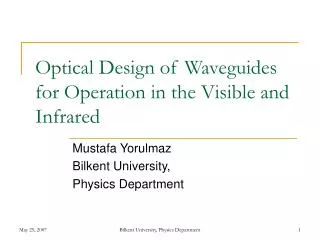
Optical Design of Waveguides for Operation in the Visible and Infrared Mustafa Yorulmaz Bilkent University, Physics Department Bilkent University, Physics Department
Outline • Waveguide theory • Simulation Methodology • State-of-the-art of rib-waveguides • Our rib-waveguide designs • State-of-the art of slot-waveguides • Our slot-waveguide design • Achievements Bilkent University, Physics Department
Planar mirror waveguides Wave-fronts and raypaths The picture shows the wave-fronts in addition to the ray model. In order to have constructive interference, the twice reflected wave must be in phase with the incident wave: The angle of inclination is discrete, only a limited number of angles are permitted for constructive interference. Bilkent University, Physics Department
The number of modes of a waveguide is limited It is derived that the angle of inclination is discrete: since The total number of modes is M, which is a function of waveguide thickness and the wavelength. If 2d/λ<1 no modes available thus λmax=2d or fmin=c/2d (cut-off frequency). If M=1, i.e. 1<2d/λ<2 then the wave guide is called single-mode Example: If d=0.5μ, the cut-off wavelength is 1μ. The waveguide is single-mode for wavelengths down to 0.5μ, and multi-mode for lower wavelength operations. Bilkent University, Physics Department
Planar Dielectric Waveguides Field distributions for TE guided modes in a dielectric waveguide. The condition for total internal reflection: The condition for constructive interference: Bilkent University, Physics Department
Optical coupling Light propagates in a waveguide in the form of modes, the complex amplitude of the Electric field is the superposition of these modes: αm is amplitude, um(y) is transverse distribution The amplitude of different modes depend on the light source used to “excite” the waveguide. If the source has a distribution that matches perfectly that of a specific mode, only that mode is excited. A source of arbitrary distribution excites different modes by different amounts. The amplitude of the lth mode is found by the overlap integral of the lth mode and the light distributions s(y) Bilkent University, Physics Department
Simulation methodology The geometrical structure and the piecewise constant n(x,y) profile, makes analytical solutions of field distributions very difficult. Numerical methods provide reliable approximate solutions. Finite Difference Method: the structure is divided into cells so that inside the cell the refractive index is constant. The differential operator is replaced by: Rib waveguide Bilkent University, Physics Department
Simulation program • Waveguide Mode Solver by Hilmi Volkan Demir and Vijit Sabnis • Finite difference method (FDM) • Solving the polarised solutions of the wave equation. Geometry of rib-waveguide structure Cell structure of finite difference scheme Inputs and outputs of the simulation program Bilkent University, Physics Department
Structure of their design and our simulation results to their structure -Single mode -Power coupling efficiency is 0.81 -Active region overlap integral is 0.99 -It lacks of MQWs Rib-waveguide structure presented in * Parameters of rib-waveguide structure presented in * Our simulation result to the structure presented in * * R. Hui, Y. Wan, J. Li, S. X. Jin, J. Y. Lin, and H. X. Jiang, “III-nitride-based planar lightwave circuits for long wavelength optical communications,” IEEE J. Quantum Electron. 41, 100-110 (2005). Bilkent University, Physics Department
Structure of their design and our simulation results to their structure Rib-waveguide structure presented in ** Our simulation result to the structure presented in ** -It has MQWs -E-field distribution doesn’t project on active layer -It has a rib-widht smaller than 1um -Power coupling efficiency is 0.6 -Active region overlap integral is 0.001 Parameters of rib-waveguide structure presented in ** ** T. N. Oder, J. Y. Lin and H. X. Jiang, “Propagation Properties of Light in AlGaN/GaN Quantum Well Waveguides.” Appl. Phy. Lett. 79, 2511 (2001). Bilkent University, Physics Department
Challenges for Design • Rib-width > 1mm for fabrication • Single mode • Having MQWs • Circular mode profile • Material overlap integral • Coupling Efficiency Bilkent University, Physics Department
Our design @1550nm Our rib-waveguide design structure for IR region, E-field distribution of this structure -MQWs are designed as ten periods of AlN(1.2nm)/GaN(1.4nm) layers. -The rib has a width of 2.5µm -Rib-width is 2.5 um > 1um -Single mode operation -Made of MWQs -Circular mode profile -Power coupling efficiency is 0.078 -Active region overlap integral is 0.05 Parameters of our rib-waveguide structure for IR region Bilkent University, Physics Department
Our design @440nm Our rib-waveguide design structure for IR region, E-field distribution of this structure -MQWs are designed as five periods of In35Ga65N(4nm)/GaN(4nm) layers. -Rib-width is 1.5 um > 1um -Single mode operation -Made of MWQs -Circular mode profile -Power coupling efficiency is 0.074 -Active region overlap integral is 0.13 Parameters of our rib-waveguide structure for IR region Bilkent University, Physics Department
Achievements with our rib-waveguide designs • Having MQWs • Satisfying single mode operation • Rib width > 1mm (@440nm and @1550nm) • Power coupling ~ 0.7-0.8 (@440nm and @1550nm) • Material Overlap > 0.1 (@440nm) Bilkent University, Physics Department
New type of waveguide design: Slot-waveguide • Different way for confining and enhancing light: Guiding light in low-index materials • According to the Maxwell’s laws that the electric field must undergo a large discontinuity with much higher amplitude in the low index side to satisfy the continuity of the normal component of electric flux density for a high-index-contrast interface. So that, this discontinuity is used to strongly enhance and confine light in a nanometer-wide region of low index material • Parameters • nc • ns • nh • wh • ws • h Geometry of slot-waveguide structure presented *** *** V. Almeida, Q. Xu, C. Barrios, and M. Lipson, “Guiding and confining light in void nanostructure,” Opt. Lett. 29, 1209 (2004) . [ISI] . Bilkent University, Physics Department
Verification of paper for slot-waveguide design Parameters and geometry of slot-waveguide structure presented in *** The contours of E-field amplitude and E-field lines that are shown in***. 3D surface plot of E-field amplitudes presented in *** Our simulation results to the structure presented in *** -In this study, we confirm the result of paper [***] and we also calculate power coupling efficiency and active region overlap integral of their structure. They are 0.63 and 0.65 respectively. *** V. Almeida, Q. Xu, C. Barrios, and M. Lipson, “Guiding and confining light in void nanostructure,” Opt. Lett. 29, 1209 (2004) . [ISI] . Bilkent University, Physics Department
Our-slot waveguide design for operation @ 1550nm -We obtained our slot-waveguide-design made of AlN -Single-mode operation -At nano-meter scale -Important for future integration of waveguides in optoelectronic and photonic devices -Power coupling efficiency is 0.8 and active region overlap integral is 0.48 of this slot-waveguide Bilkent University, Physics Department
Thanks.. Questions? Bilkent University, Physics Department