Download
1 / 47
470 likes | 640 Vues
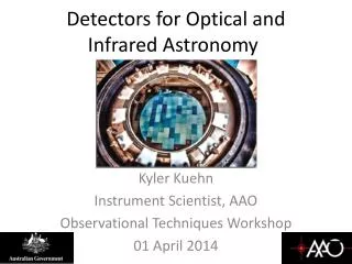
Detectors for Optical and Infrared Astronomy . Kyler Kuehn Instrument Scientist, AAO Observational Techniques Workshop 01 April 2014. The Dark Energy Camera.

E N D
Detectors for Optical and Infrared Astronomy Kyler Kuehn Instrument Scientist, AAO Observational Techniques Workshop 01 April 2014
The Dark Energy Camera 62 2k x 4k full-frame, fully-depleted, backside-illuminated, 4-side-buttable, dual-readout, p-channel LBNL CCDs with 250 micron x 15 micron x 15 micron pixels, possessing 130ke- fullwell, 2.5 ADU/e- gain, “five nine” CTE, totaling 520 Megapixels with >50% QE from 375 nm to 1000 nm, operating at 173K, with an overall FOV of 3 sq deg.
Motivation • For some of you, astronomical images and spectra are things that from time to time show up on your screen and/or in your hard drive as FITS files. • If the materials scientists and optical engineers (and software engineers, and…) have done their job properly, you generally won’t have to worry about most of the details in this presentation. • But it can be useful to know what’s “under the hood”, so you can (at least) understand the motivations behind each data analysis step, and (possibly) identify and contribute to the resolution of issues arising from your own observations.
Detectors: a History (in one slide) Unaided human eye: Area ~40 mm2, “Integration time” ~0.04 s cf. Rudolphine Tables (data acquired by Tycho Brahe up to 1601, published by Kepler in 1627) First telescopes (circa 1608): <700mm2 (though with significant aberration) Galileo’s drawing of Jupiter’s “Medicean Stars”: Cosimo, Francesco, Carlo and Lorenzo Sources: Brahe’s Mechanica, Galileo’s telescope from Florence’s Museo Galilei, Image from Sidereus Nuncius
(OK, make that two slides) Photographic Plates: • Gelatin film (usually) containing light-sensitive silver salts, activated by incident light then chemically “fixed” to prevent further change • Glass plates do not deform like photographic film does • Area, resolution, & integration time limited primarily by the opto-mechanical precision of telescope and instruments • Drawbacks: low QE (2% vs. 90%), non-linear response, processing of data is challenging Source: UKST Southern Sky Survey (IoA, Cambridge)
Charge-Coupled Devices • Photons converted to electronic signal via the photoelectric effect • CCD comprises an array of pixels, acting as “light buckets” • Shift register reads out pixel values by “clocking” the gate voltage, “bucket bridgade”-style • For sensitivity to optical wavelengths, detectors are silicon, doped with B or P • Contain a lattice of overlapping Si e- orbitals • Individual e- can be dissociated from the lattice by an incident photon and conducted to the pixel electrode Smith & Boyle shared (half of) the Nobel Prize in 2009 for the invention of the CCD.
CCD Fabrication • Start* with bare Si wafer • Slicing, polishing • Thinning • Doping • Plasma etching • Chemical vapor deposition • Photolithography • Dicing • Packaging • Testing Source: LBNL * There’s a whole talk hidden in this one word too.
A Single CCD Picture Element (Pixel) Fully Depleted Deeply Depleted Source: Dark Energy Survey/LBNL
CCD Quantum Efficiency GMOS-S (Hamamatsu Red/Blue CCDs)
Non-Imaging Regions of a CCD Source: LBNL
Voltage Bus Imaging Array Vertical Clock Voltages Channel Stop Shift Register Source: FNAL Silicon Detector Facility (Gordie Gillespie)
Charge Transfer (In)Efficiency Standard CCDs usually have 99.999% (“five nines”) charge transfer efficiency in the shift register. That sounds pretty good, but… (0.99999)(4096+1024) = 95% (0.999999)(4096+1024) = 99.5% Six nines is significantly better!
Noise Characteristics: Bias Voltage GMOS-N CCDs A baseline voltage is applied to all pixels so that all random noise is by definition positive. But this requires subtracting this “base level” read noise from all science-related exposures. Bias frames can also be used to identify the effects of some physical defects in the CCD.
Depletion Fraction/Voltage Effects 650 μm thick CCD 200 μm thick CCD Not fully depleted at 100V Fully depleted at 100V Source: LBNL
CCD Cold-Probe Testing at FNAL Source: FNAL Silicon Detector Facility
Errors Arising from CCD Fabrication • Tape bumps (from physical assembly process) • Glowing edges (e- γ in amplifier near pixels) • Hot spots (substrate voltage leakage) • Bad pixels (the “bucket” has a hole…) • Bad columns (“traps” – the voltage or shift register connection is broken) • And many more….
From Pixels to CCDs: Choices • Will you be taking images or spectra? • Do you want a full frame CCD (needs mechanical shutter) or a frame transfer CCD (faster readout, but 1/2 active Si area)? Do you want front- or back-side illumination? • How thick is your photoactive region (i.e., how red-sensitive)? Do you want deep/full depletion? • Does your telescope track (non-)sidereal objects, or do you observe in drift scan mode? For the latter, your readout must be aligned precisely with the scan direction. • Do you want to cool your instrument? To what temperature -- do you need a cryogenic system or will thermoelectric cooling provide sufficiently low dark current? • What wavelength region will you observe? What detector material and A/R coating will you use? • What size pixels do you require in microns, and in arcseconds on the sky (the “plate scale”) given your telescope optics? Are you over- or under-sampling (2 * pixel scale > minimum seeing)? • What field of view do you want to cover in an exposure? How many CCDs will be in your detector? How close do they need to be? This determines whether to use picture frame or 2-side buttable or 4-side buttable devices. • What level of cosmetic defects will hamper your science? What voltages can the silicon withstand? • Your readout likely saturates at 65535 (216 – 1 for a 16 bit system); what fullwell capacity (between say, 100ke- to 300 ke-) is optimal? What is the requisite gain? • At what stage does saturation/non-linearity begin to affect your measurements?
Source: Dark Energy Survey/ LBNL
Fabricating Devices is Tricky! Device Yield Fabrication: 80% (“Mechanical CCDs”) Cosmetic Defects/ Cold-Probe Tests: 60% (“Engineering CCDs”) “Science Grade”: <25% Source: DES/FNAL
The finished product (sort of) Source: DES/FNAL
CCD Focal Plane Installation Source: DES/FNAL
Instrument Installation Source: DES/CTIO
Data Acquisition (DAQ) IRAF/IDL (and even cfitsio) are still far away. Between the shift register and the image is the DAQ For example: Monsoon crate containing Clock & Bias Boards, Master Control Boards Also, the electronic signal may be turned back into photons via S-Link fibre optic cable to the data PC. Then telescope/observation control and telemetry data are added Then you have a (FITS) file with pixel array data and header information Then you can test your on-sky performance ASIC Readout for SNAP Source: LBNL
Fullwell/Saturation (~120ke- = 65535 ADU?) Fullwell degradation from over-exposure? Gain (ADU/e-) Linearity (fraction of FW?) Shutter Vignetting Source: DES/PreCam
Shutter Vignetting, Saturation Source: DES/PreCam
Dark Current • Integrate for the same amount of time as a science exposure, but with the shutter closed. • This determines the (thermal) noise rate that is then subtracted from each pixel. • Cryogenic cooling to ~173K is common for many astronomical instruments, some can get away with 183 or warmer without swamping the detectors with thermal noise.
Flat Fielding Pixel-to-pixel variation in (quantum) efficiency means uniform illumination will not result in uniform counts from every pixel Thus we divide each science image by a flat field image so that a pixel with, say, 2x the efficiency is weighted by ½ relative to the others. Dipoles? AAT Wide Field Imager + Prime Focus Unit in z band
Fringing Scattered light from within the CCD, especially noticeable in redder wavelengths GMOS-S CCDs
Cosmic Rays Source: DES/PreCam
What’s the source of this noise? Spoiler: readout cable/pin connector micro-fractures resulting in intermittent additive (common mode?) noise Source: DES/PreCam
Sources of Counts in a Pixel • Read Noise (Hopefully subtracted properly) • Dark Current (Hopefully subtracted properly) • Sky Noise (Ambient and Anthropogenic) • Scattered light/ghosting (LEDs in instrument)? • Photons from a source (Signal + Shot Noise) • Signal to Noise calculators take all of these (as well as system throughput) and determine exposure times • This feeds into observing proposals…
TAIPAN: A Case Study Includes: Spectral Cross-Contamination CCD QE Spectrograph Optics/Coatings Fibre Output/Connector Fibre Length Fibre Injection Loss Fibre Alignment Interface Thermal Aberration Focal Plane Thermal Aberration Focal Plane Optics Vignetting Telescope Optics Atmosphere
TAIPAN: A Case Study From Survey Requirements through Exposure Time Calculator to CCD Specifications • Magnitude 18 galaxy with S/N ~10 in 2.5 hours • Magnitude 12 star with S/N ~100 in 2.5 minutes • Long exposures for faint objects • Short exposures for bright objects • Medium exposures for medium objects • Under what conditions do Read Noise, Dark Current, Sky Noise, or Shot Noise dominate? • TAIPAN Requirements: • Read Noise < 3 e-/pix • Dark Current < 0.01 e-/pix/s
Other Detector Technologies • HgCdTe (“MerCadTel”): IR-sensitive (1.5-12 um) detectors. • Hawaii 2-RG detectors (e.g. in the Gemini Planet Imager) have a (non-destructive!) readout layer made of Si. • Thermal noise (infrared photons) is more of an issue, requiring high-performance cryogenic cooling. • Much of what has been described here for Si is applicable to HgCdTe. • InSb (e.g., ESO’s ALADDIN sensor arrays on VLT), or InGaAs • Photomultiplier tubes (“avalanche” detectors) • Electron Multiplying Charge-Coupled Device (Si CCD with increased Gain like PMT, cf. NuVu Cameras) • Other wavelengths? (gamma, X, UV, microwave, radio) • Other astrophysical messengers? (neutrinos, gravitational) • Microwave Kinetic Inductance Detectors (MKIDs)…
The Future(?): MKIDS LC Circuit gives energy and timing information of individual photons but requires (even more) sophisticated readout and precise cooling than a standard Si-based device Source: Mazin Lab (http://web.physics.ucsb.edu/~bmazin/Mazin_Lab/MKIDs.html)
The Dark Energy Camera 62 2k x 4k full-frame, fully-depleted, backside-illuminated, 4-side-buttable, dual-readout, p-channel LBNL CCDs with 250 micron x 15 micron x 15 micron pixels, possessing 130ke- fullwell, 2.5 ADU/e- gain, “five nine” CTE, totaling 520 Megapixels with >50% QE from 375 to 1000 nm, operating at 173K, with an overall FOV of 3 sq deg.
Only after this entire process can your detectors obtain results like this: Coma Cluster; Source: DES
Or this: NGC 1365; Source: DES
Thank You! Source: Marcelle Soares-Santos, FNAL
Useful References • AY257 Modern Observational Techniques http://www.ucolick.org/~bolte/AY257/s_n.pdf • Dark Energy Survey Instrumentation http://www.darkenergysurvey.org/DECam/ (see also http://www.ctio.noao.edu/noao/content/DECam-Known-Problems) • Mazin Lab http://web.physics.ucsb.edu/~bmazin/Mazin_Lab/MKIDs.html • Gemini Instrumentation http://www.gemini.edu/node/10002 • Me (Follow up questions? Want more details?) kkuehn@aao.gov.au • Wikipedia/Amazon (no kidding)