Download

1 / 16
170 likes | 324 Vues
Scaling of a controller for an active filter. Procedure. Design controller and identify physical controller Introduce model of various signal and variable Group gains and offsets, scaling variables Implement multiplications with shift operator. A rectifier. Given: U mains sinusoidal

E N D
Procedure • Design controller and identify physical controller • Introduce model of various signal and variable • Group gains and offsets, scaling variables • Implement multiplications with shift operator
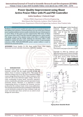
A rectifier Given: Umainssinusoidal Objective: Imains sinusoidal in phase with Umains and with given amplitude Measurements: Imains and Umains UDC/2 Imains Umains UDC/2
Ideal controller for rectifier with given reference current feedback term controller I mains - + Sinus K Rif. LC + + I mains reference current U mains feedforward term
1 U M Ideal controller with reference currentproportional to mains voltage (UM is maximal allowable voltage) Physical system DSP code I mains - + Sinus K Rif. LC LC + + I mains U mains Ref.I.
conversiongain fromsensor inverse gain 1 U M Introduce gain of Hall sensor (LEM) givingend-scale voltage ULEM for end-scale current IM LEM U I LEM M I U LEM M I mains - + Sinus K Rif. LC LC + + I RETE U mains Ref.I.
U I LEM M I U LEM M U 1 U M DSP U U U M DSP M Introduce gain of analog electronics adapting output voltage range of sensor (2*ULEM) to input voltage range of AD converter (2*UDSP), same for voltage measurement LEM U U LEM DSP U U DSP LEM I mains - + Sinus K Rif. LC LC + + I mains U mains Ref.I.
U U U U DSP DSP DSP DSP - - + + U U U + + I + + LEM LEM DSP M U U I U LEM DSP M LEM U 1 U M DSP U U U M DSP M Introduce offset of analog electronics adapting output voltage level of sensor (-ULEM ULEM) to input voltage level of AD converter (02*UDSP), same for voltage measurement Interface board LEM I msina - + Sinus K Rif. LC LC + + I mains U mains Ref.I. Interface board
U U U I × 2 U BIT LEM LEM DSP M DSP IN × U 2 U U I U BIT DSP IN LEM DSP M LEM U 1 × U 2 U BIT M DSP DSP IN × BIT 2 U U U U DSP IN M DSP M Introduce AD conversion from DSP inputvoltages (0 2*UDSP ) to AD register values (0BITIN) Interface board U U DSP LEM DSP AD - + + + I msina - + Sinus K Rif. LC LC + + I mains U mains U U DSP DSP AD - + + + Ref.I. Interface board
U U U I × 2 U BIT LEM LEM DSP M DSP IN × U 2 U U I U BIT DSP IN LEM DSP M LEM × BIT 2 U OUT DC × 2 U BIT DC OUT BIT BIT OUT OUT 2 2 U 1 × U 2 U BIT M DSP DSP IN × BIT 2 U U U U DSP IN M DSP M Add PWM gain from register range (0 BITout) to average output voltage range (-UDC UDC) and add offset of register (BITout/2) Interface board U U DSP LEM DSP AD - + + + I mains PWM-DSP - + + Sinus + K Rif. LC LC + + + - I mains U mains U U DSP DSP AD - + + + Ref.I. Interface board
- - + + K ×IM U UM DSP - U U U 2 × UM I 2 × UM 2 × UM 2 × IM + × × × × × 2 2 2 2 2 U U U IM ×K IM ×K BIT LEM LEM DSP M DSP DSP DSP IN × U 2 U U I BIT BIT U BIT 2 × UM BIT BIT BIT BIT BIT BIT DSP IN IN IN IN IN IN IN LEM IN IN DSP M LEM × BIT BIT BIT 2 U OUT OUT OUT DC BITIN × × 2 2 U U BIT DC DC 2 × UM OUT BIT BITIN BIT BITIN OUT OUT 2 2 BITIN× Ref.I. 2 × IM ×UM Ref.I. Ref.I. U M IM U 1 × U 2 U BITIN× Ref.I. BIT M DSP DSP IN 2 × IM ×UM × BIT 2 U U U U DSP IN M DSP M Choose signed integer format, leave offset close to converters, move gains to maintain variable sizes as much as possible as size of measurement (registers range) interface board U LEM DSP AD + + I mains PWM-DSP - + + Sinus + K Rif. LC + + + - I mains U mains U U DSP DSP AD - + + + Ref.I. interface board
Use shift operator Operation Y=X*0.51= (X*0.51*1024)/1024 (X*522)/1024 implemented as Y=(X*522) >> 10 because 1024=210